JAJSDH0J April 2008 – June 2017 LM5118
PRODUCTION DATA.
- 1 特長
- 2 アプリケーション
- 3 概要
- 4 改訂履歴
- 5 Pin Configuration and Functions
- 6 Specifications
- 7 Detailed Description
-
8 Application and Implementation
- 8.1 Application Information
- 8.2
Typical Application
- 8.2.1 Design Requirements
- 8.2.2
Detailed Design Procedure
- 8.2.2.1 Custom Design With WEBENCH® Tools
- 8.2.2.2 R7 = RT
- 8.2.2.3 Inductor Selection, L1
- 8.2.2.4 R13 = RSENSE
- 8.2.2.5 C15 = CRAMP
- 8.2.2.6 Inductor Current Limit Calculation
- 8.2.2.7 C9 - C12 = Output Capacitors
- 8.2.2.8 D1
- 8.2.2.9 D4
- 8.2.2.10 C1 - C5 = Input Capacitor
- 8.2.2.11 C20
- 8.2.2.12 C8
- 8.2.2.13 C16 = CSS
- 8.2.2.14 R8, R9
- 8.2.2.15 R1, R3, C21
- 8.2.2.16 R2
- 8.2.2.17 Snubber
- 8.2.2.18 Error Amplifier Configuration
- 8.2.3 Application Curves
- 9 Power Supply Recommendations
- 10Layout
- 11デバイスおよびドキュメントのサポート
- 12メカニカル、パッケージ、および注文情報
パッケージ・オプション
メカニカル・データ(パッケージ|ピン)
- PWP|20
サーマルパッド・メカニカル・データ
- PWP|20
発注情報
10 Layout
10.1 Layout Guidelines
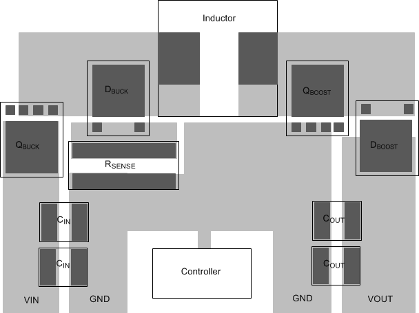
In a buck-boost regulator, there are two loops where currents are switched very fast. The first loop starts from the input capacitors, and then to the buck switch, the inductor, the boost switch then back to the input capacitor. The second loop starts from the inductor, and then to the output diode, the output capacitor, the re-circulating diode, and back to the inductor. Minimizing the PCB area of these two loops reduces the stray inductance and minimizes noise and the possibility of erratic operation. A ground plane in the PCB is recommended as a means to connect the input filter capacitors to the output filter capacitors and the PGND pins of the LM5118. Connect all of the low current ground connections (CSS, RT, CRAMP) directly to the regulator AGND pin. Connect the AGND and PGND pins together through topside copper area covering the entire underside of the device. Place several vias in this underside copper area to the ground plane of the input capacitors.
10.2 Layout Example
 Figure 29. LM5118 Layout Example