JAJSE53 September 2017 LM73605 , LM73606
PRODUCTION DATA.
- 1 特長
- 2 アプリケーション
- 3 概要
- 4 改訂履歴
- 5 Pin Configuration and Functions
- 6 Specifications
-
7 Detailed Description
- 7.1 Overview
- 7.2 Functional Block Diagram
- 7.3
Feature Description
- 7.3.1 Synchronous Step-Down Regulator
- 7.3.2 Auto Mode and FPWM Mode
- 7.3.3 Fixed-Frequency Peak Current-Mode Control
- 7.3.4 Adjustable Output Voltage
- 7.3.5 Enable and UVLO
- 7.3.6 Internal LDO, VCC_UVLO, and BIAS Input
- 7.3.7 Soft Start and Voltage Tracking
- 7.3.8 Adjustable Switching Frequency
- 7.3.9 Frequency Synchronization and Mode Setting
- 7.3.10 Internal Compensation and CFF
- 7.3.11 Bootstrap Capacitor and VBOOT-UVLO
- 7.3.12 Power-Good and Overvoltage Protection
- 7.3.13 Overcurrent and Short-Circuit Protection
- 7.3.14 Thermal Shutdown
- 7.4 Device Functional Modes
-
8 Application and Implementation
- 8.1 Application Information
- 8.2
Typical Application
- 8.2.1 Design Requirements
- 8.2.2
Detailed Design Procedure
- 8.2.2.1 Custom Design With WEBENCH® Tools
- 8.2.2.2 Output Voltage Setpoint
- 8.2.2.3 Switching Frequency
- 8.2.2.4 Input Capacitors
- 8.2.2.5 Inductor Selection
- 8.2.2.6 Output Capacitor Selection
- 8.2.2.7 Feed-Forward Capacitor
- 8.2.2.8 Bootstrap Capacitors
- 8.2.2.9 VCC Capacitor
- 8.2.2.10 BIAS
- 8.2.2.11 Soft Start
- 8.2.2.12 Undervoltage Lockout Setpoint
- 8.2.2.13 PGOOD
- 8.2.3 Application Curves
- 9 Power Supply Recommendations
- 10Layout
- 11デバイスおよびドキュメントのサポート
- 12メカニカル、パッケージ、および注文情報
パッケージ・オプション
メカニカル・データ(パッケージ|ピン)
- RNP|30
サーマルパッド・メカニカル・データ
- RNP|30
発注情報
6 Specifications
6.1 Absolute Maximum Ratings
Over operating free-air temperature range of –40°C to +125°C (unless otherwise noted)(1)| PARAMETER | MIN | MAX | UNIT | |
|---|---|---|---|---|
| Input voltages | PVIN to PGND | –0.3 | 42 | V |
| EN to AGND | –0.3 | VIN + 0.3 | ||
| FB, RT, SS/TRK to AGND | –0.3 | 5 | ||
| PGOOD to AGND | –0.1 | 20 | ||
| SYNC to AGND | –0.3 | 5.5 | ||
| BIAS to AGND | –0.3 | Lower of (VIN + 0.3) or 20 | ||
| AGND to PGND | –0.3 | 0.3 | ||
| Output voltages | SW to PGND | –0.3 | VIN + 0.3 | V |
| SW to PGND less than 10-ns transients | –3.5 | 42 | ||
| CBOOT to SW | –0.3 | 5 | ||
| VCC to AGND | –0.3 | 5 | ||
| Operating junction temperature, TJ | –40 | 150 | °C | |
| Storage temperature, Tstg | –65 | 150 | °C | |
(1) Stresses beyond those listed under Absolute Maximum Ratings may cause permanent damage to the device. These are stress ratings only, which do not imply functional operation of the device at these or any other conditions beyond those indicated under Recommended Operating Conditions. Exposure to absolute-maximum-rated conditions for extended periods may affect device reliability.
6.2 ESD Ratings
| VALUE | UNIT | |||
|---|---|---|---|---|
| V(ESD) | Electrostatic discharge | Human-body model (HBM), per ANSI/ESDA/JEDEC JS-001(1) | ±2000 | V |
| Charged-device model (CDM), per JEDEC specification JESD22-C101(2) | ±750 | |||
(1) JEDEC document JEP155 states that 500-V HBM allows safe manufacturing with a standard ESD control process.
(2) JEDEC document JEP157 states that 250-V CDM allows safe manufacturing with a standard ESD control process.
6.3 Recommended Operating Conditions
Over operating free-air temperature range of –40°C to +125°C (unless otherwise noted)(1)| MIN | MAX | UNIT | ||
|---|---|---|---|---|
| Input voltages | PVIN to PGND | 3.5 | 36 | V |
| EN | 0 | VIN | ||
| FB | 0 | 4.5 | ||
| PGOOD | 0 | 18 | ||
| BIAS input not used | 0 | 0.3 | ||
| BIAS input used | 0 | Lower of (VIN + 0.3) or 18 | ||
| AGND to PGND | –0.1 | 0.1 | ||
| Output voltage | VOUT | 1 | 95% of VIN | V |
| Output current | IOUT, LM73605 | 0 | 5 | A |
| IOUT, LM73606 | 0 | 6 | A | |
| Temperature | Operating junction temperature, TJ | –40 | 125 | °C |
(1) Recommended operating rating indicate conditions for which the device is intended to be functional, but do not ensure specific performance limits. For ensured specifications, see Electrical Characteristics
6.4 Thermal Information
| THERMAL METRIC(1) | LM73605/LM73606 | UNIT | |
|---|---|---|---|
| RNP (WQFN) | |||
| 30 PINS | |||
| RθJA | Junction-to-ambient thermal resistance | 34.3 | °C/W |
| RθJC(top) | Junction-to-case (top) thermal resistance | 14.6 | °C/W |
| RθJB | Junction-to-board thermal resistance | 7.3 | °C/W |
| ψJT | Junction-to-top characterization parameter | 0.1 | °C/W |
| ψJB | Junction-to-board characterization parameter | 7.1 | °C/W |
| RθJC(bot) | Junction-to-case (bottom) thermal resistance | 1 | °C/W |
(1) For more information about traditional and new thermal metrics, see the Semiconductor and IC Package Thermal Metrics application report.
6.5 Electrical Characteristics
Limits apply over the recommended operating junction temperature (TJ) range of –40°C to +125°C, unless otherwise stated. Minimum and maximum limits are specified through test, design or statistical correlation. Typical values represent the most likely parametric norm at TJ = 25°C, and are provided for reference purposes only. Unless otherwise stated, VIN = 12 V.| PARAMETER | TEST CONDITIONS | MIN | TYP | MAX | UNIT | |
|---|---|---|---|---|---|---|
| SUPPLY VOLTAGE (PVIN PINS) | ||||||
| VIN | Operating input voltage range | 3.5 | 36 | V | ||
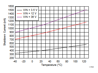
| ISD | Shutdown quiescent current; measured at VIN pin(1) | VEN = 0 V TJ = 25℃ |
0.8 | 10 | µA | |
| IQ_NONSW | Operating quiescent current from VIN (non-switching) | VEN = 2 V, VFB = 1.5 V, VBIAS = 3.3 V external | 0.6 | 12 | µA | |
| ENABLE (EN PIN) | ||||||
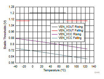
| VEN_VCC_H | Enable input high level for VCC output | VEN rising | 1.15 | V | ||
| VEN_VCC_L | Enable input low level for VCC output | VEN falling | 0.3 | V | ||
| VEN_VOUT_H | Enable input high level for VOUT | VEN rising | 1.14 | 1.196 | 1.25 | V |
| VEN_VOUT_HYS | Enable input hysteresis for VOUT | VEN falling hysteresis | –100 | mV | ||
| ILKG_EN | Enable input leakage current | VEN = 2 V | 1.4 | 200 | nA | |
| INTERNAL LDO (VCC PIN, BIAS PIN) | ||||||
| VCC | Internal VCC voltage | PWM operation | 3.27 | V | ||
| PFM operation | 3.1 | V | ||||
| VCC_UVLO | Internal VCC undervoltage lockout | VCC rising | 2.96 | 3.14 | 3.27 | V |
| VCC falling hysteresis | –605 | mV | ||||
| VBIAS_ON | Input changeover | VBIAS rising | 3.09 | 3.25 | V | |
| VBIAS falling hysteresis | –63 | mV | ||||
| IBIAS_NONSW | Operating quiescent current from external VBIAS (non-switching) | VEN = 2 V, VFB = 1.5 V, VBIAS = 3.3 V external | 21 | 50 | µA | |
| VOLTAGE REFERENCE (FB PIN) | ||||||
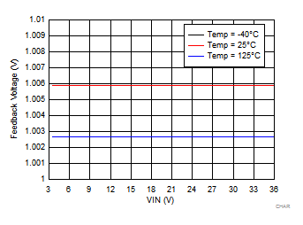
| VFB | Feedback voltage | PWM mode | 0.987 | 1.006 | 1.017 | V |
| ILKG_FB | Input leakage current at FB pin | VFB = 1 V | 0.2 | 60 | nA | |
| HIGH SIDE DRIVER (CBOOT PIN) | ||||||
| VCBOOT_UVLO | CBOOT - SW undervoltage lockout | 1.6 | 2.2 | 2.7 | V | |
| CURRENT LIMITS AND HICCUP | ||||||
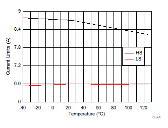
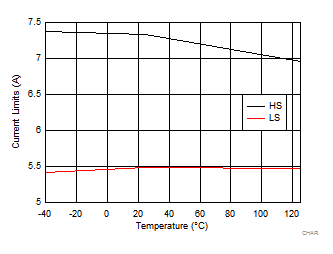
| IHS_LIMIT | Short-circuit, high-side current limit(2) | LM73605 | 6 | 7.3 | 8.35 | A |
| LM73606 | 7.4 | 8.7 | 9.85 | |||
| ILS_LIMIT | Low-side current limit(2) | LM73605 | 4.79 | 5.5 | 6.1 | A |
| LM73606 | 5.8 | 6.6 | 7.25 | |||
| INEG_LIMIT | Negative current limit | LM73605 | –5 | A | ||
| LM73606 | –6 | |||||
| VHICCUP | Hiccup threshold on FB pin | 0.36 | 0.4 | 0.44 | V | |
| IL_ZC | Zero cross-current limit | 0.06 | A | |||
| SOFT START (SS/TRK PIN) | ||||||
| ISSC | Soft-start charge current | 1.8 | 2 | 2.2 | µA | |
| RSSD | Soft-start discharge resistance | UVLO, TSD, OCP, or EN = 0 | 1 | kΩ | ||
| POWER GOOD (PGOOD PIN) and OVERVOLTAGE PROTECTION | ||||||
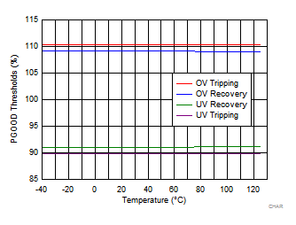
| VPGOOD_OV | Power-good overvoltage threshold | % of FB voltage | 106% | 110% | 113% | |
| VPGOOD_UV | Power-good undervoltage threshold | % of FB voltage | 86% | 90% | 93% | |
| VPGOOD_HYS | Power-good hysteresis | % of FB voltage | 1.2% | |||
| VPGOOD_VALID | Minimum input voltage for proper PGOOD function | 50-µA pullup to PGOOD pin, VEN = 0 V, TJ = 25°C | 1.3 | 2 | V | |
| RPGOOD | Power-good ON-resistance | VEN = 2.5V | 40 | 100 | Ω | |
| VEN = 0 V | 30 | 90 | ||||
| MOSFETS | ||||||
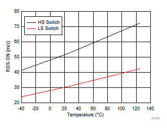
| RDS_ON_HS (3) | High-side MOSFET ON-resistance | IOUT = 1 A, VBIAS = VOUT = 3.3 V | 53 | 90 | mΩ | |
| RDS_ON_LS (3) | Low-side MOSFET ON-resistance | IOUT = 1 A, VBIAS = VOUT = 3.3 V | 31 | 55 | mΩ | |
| THERMAL SHUTDOWN | ||||||
| TSD (4) | Thermal shutdown threshold | Shutdown threshold | 160 | °C | ||
| Recovery threshold | 135 | °C | ||||
(1) Shutdown current includes leakage current of the switching transistors.
(2) This current limit was measured as the internal comparator trip point. Due to inherent delays in the current limit comparator and drivers, the peak current limit measured in closed loop with faster slew rate will be larger, and valley current limit will be lower.
(3) Measured at pins
(4) Ensured by design
6.6 Timing Characteristics
| MIN | NOM | MAX | UNIT | |||
|---|---|---|---|---|---|---|
| CURRENT LIMITS AND HICCUP | ||||||
| NOC (1) | Number of switching cycles before hiccup is tripped | 128 | Cycles | |||
| tOC | Overcurrent hiccup retry delay time | 46 | ms | |||
| SOFT START (SS/TRK PIN) | ||||||
| tSS | Internal soft-start time | CSS = OPEN, from EN rising edge to PGOOD rising edge | 3.5 | 6.3 | ms | |
| POWER GOOD (PGOOD PIN) and OVERVOLTAGE PROTECTION | ||||||
| tPGOOD_RISE | PGOOD rising edge deglitch delay | 80 | 140 | 200 | µs | |
| tPGOOD_FALL | PGOOD falling edge deglitch delay | 80 | 140 | 200 | µs | |
(1) Ensured by design
6.7 Switching Characteristics
| PARAMETER | TEST CONDITIONS | MIN | TYP | MAX | UNIT | |
|---|---|---|---|---|---|---|
| PWM LIMITS (SW PINS) | ||||||
| tON-MIN | Minimum switch on-time | 60 | 82 | ns | ||
| tOFF-MIN | Minimum switch off-time | 70 | 120 | ns | ||
| tON-MAX | Maximum switch on-time | HS timeout in dropout | 3 | 6 | 9 | µs |
| OSCILLATOR (RT and SYNC PINS) | ||||||
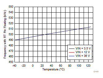
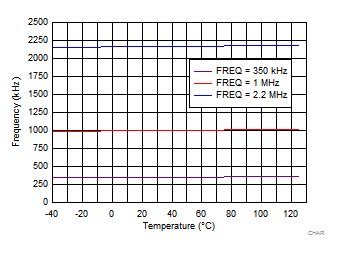
| fOSC | Internal oscillator frequency | RT = Open | 440 | 500 | 560 | kHz |
| fADJ | Minimum adjustable frequency by RT or SYNC | RT =115 kΩ, 0.1% | 315 | 350 | 385 | kHz |
| Maximum adjustable frequency by RT or SYNC | RT = 17.4 kΩ, 0.1% | 1980 | 2200 | 2420 | kHz | |
| VSYNC_HIGH | Sync input high level threshold | 2 | V | |||
| VSYNC_LOW | Sync input low level threshold | 0.4 | V | |||
| VMODE_HIGH | Mode input high level threshold for FPWM | 0.42 | V | |||
| VMODE_LOW | Mode input low level threshold for AUTO mode | 0.4 | V | |||
| tSYNC_MIN | Sync input minimum ON and OFF-time | 80 | ns | |||
6.8 System Characteristics
The following specifications apply to the circuit found in typical schematic with appropriate modifications from typical bill of materials. These parameters are not tested in production and represent typical performance only. Unless otherwise stated the following conditions apply: TA = 25°C, VIN = 12 V, VOUT = 3.3 V, fSW = 500 kHz.| PARAMETER | TEST CONDITIONS | MIN | TYP | MAX | UNIT | |
|---|---|---|---|---|---|---|
| VFB_PFM | Output voltage offset at no load in auto mode | VIN = 3.8 V to 36 V, VSYNC = 0 V, auto mode IOUT = 0 A | 2% | |||
| VDROP | Minimum input to output voltage differential to maintain specified accuracy | VOUT = 5 V, IOUT = 3 A, fSW = 2.2 MHz | 0.4 | V | ||
| IQ_SW | Operating quiescent current (switching) | VEN = 3.3 V, IOUT = 0 A, RT = open, VBIAS = VOUT = 3.3 V , RFBT = 1 Meg | 15 | µA | ||
| IPEAK_MIN | Minimum inductor peak current | LM73605 : VSYNC = 0, IOUT = 10 mA |
1 | A | ||
| LM73606 : VSYNC = 0 V, IOUT = 10 mA |
1.3 | |||||
| IBIAS_SW | Operating quiescent current from external VBIAS (switching) | fSW = 500 kHz, IOUT = 1 A | 7 | mA | ||
| fSW = 2.2 MHz, IOUT = 1 A | 25 | |||||
| DMAX | Maximum switch duty cycle | While in frequency foldback | 97.5% | |||
| tDEAD | Dead time between high-side and low-side MOSFETs | 4 | ns | |||
6.9 Typical Characteristics
Unless otherwise specified, VIN = 12 V. Curves represent most likely parametric norm at specified condition.