SNOS719G September 1999 – September 2015 LMC7101 , LMC7101Q-Q1
PRODUCTION DATA.
- 1 Features
- 2 Applications
- 3 Description
- 4 Revision History
- 5 Pin Configuration and Functions
-
6 Specifications
- 6.1 Absolute Maximum Ratings
- 6.2 ESD Ratings: LMC7101
- 6.3 ESD Ratings: LMC7101Q-Q1
- 6.4 Recommended Operating Conditions
- 6.5 Thermal Information
- 6.6 Electrical Characteristics: 2.7 V
- 6.7 DC Electrical Characteristics: 3 V
- 6.8 DC Electrical Characteristics: 5 V
- 6.9 DC Electrical Characteristics: 15 V
- 6.10 AC Electrical Characteristics: 5 V
- 6.11 AC Electrical Characteristics: 15 V
- 6.12 Typical Characteristics
- 7 Detailed Description
- 8 Application and Implementation
- 9 Power Supply Recommendations
- 10Layout
- 11Device and Documentation Support
- 12Mechanical, Packaging, and Orderable Information
1 Features
- Tiny 5-Pin SOT-23 Package Saves Space—Typical Circuit Layouts Take Half the Space of 8-Pin SOIC Designs
- Ensured Specifications at 2.7-V, 3-V, 5-V, 15-V Supplies
- Typical Supply Current 0.5 mA at 5 V
- Typical Total Harmonic Distortion of 0.01% at 5 V
- 1-MHz Gain Bandwidth
- Similar to Popular LMC6482 and LMC6484
- Rail-to-Rail Input and Output
- Temperature Range –40°C to 125°C
(LMC7101Q-Q1)
2 Applications
- Mobile Communications
- Notebooks and PDAs
- Battery Powered Products
- Sensor Interface
- Automotive Applications (LMC7101Q-Q1)
3 Description
The LMC7101 device is a high-performance CMOS operational amplifier available in the space-saving 5-pin SOT-23 tiny package. This makes the LMC7101 ideal for space- and weight-critical designs. The performance is similar to a single amplifier of the LMC6482 and LMC6484 types, with rail-to-rail input and output, high open-loop gain, low distortion, and low-supply currents.
The main benefits of the tiny package are most apparent in small portable electronic devices, such as mobile phones, pagers, notebook computers, personal digital assistants, and PCMCIA cards. The tiny amplifiers can be placed on a board where they are needed, thus simplifying board layout.
Device Information(1)
| PART NUMBER | PACKAGE | BODY SIZE (NOM) |
|---|---|---|
| LMC7101, LMC7101Q-Q1 |
SOT-23 (5) | 2.90 mm × 1.60 mm |
- For all available packages, see the orderable addendum at the end of the data sheet.
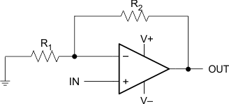
Example Application
