JAJSER4B February   2018  – October 2018 LMG1020

PRODUCTION DATA.  

  1. 特長
  2. アプリケーション
  3. 概要
    1.     Device Images
      1.      LiDARドライバ段の概略図
  4. 改訂履歴
  5. Pin Configuration and Functions
    1.     Pin Functions
  6. Specifications
    1. 6.1 Absolute Maximum Ratings
    2. 6.2 ESD Ratings
    3. 6.3 Recommended Operating Conditions
    4. 6.4 Thermal Information
    5. 6.5 Electrical Characteristics
    6. 6.6 Switching Characteristics
    7. 6.7 Typical Characteristics
  7. Detailed Description
    1. 7.1 Overview
    2. 7.2 Functional Block Diagram
    3. 7.3 Feature Description
      1. 7.3.1 Input Stage
      2. 7.3.2 Output Stage
      3. 7.3.3 VDD and undervoltage lockout
      4. 7.3.4 Overtemperature Protection (OTP)
    4. 7.4 Device Functional Modes
  8. Application and Implementation
    1. 8.1 Application Information
    2. 8.2 Typical Application
      1. 8.2.1 Design Requirements
      2. 8.2.2 Detailed Design Procedure
        1. 8.2.2.1 Handling Ground Bounce
        2. 8.2.2.2 Creating Nanosecond Pulse With LMG1020
      3. 8.2.3 VDD and Overshoot
      4. 8.2.4 Operating at Higher Frequency
      5. 8.2.5 Application Curves
  9. Power Supply Recommendations
  10. 10Layout
    1. 10.1 Layout Guidelines
      1. 10.1.1 Gate Drive Loop Inductance and Ground Connection
      2. 10.1.2 Bypass Capacitor
    2. 10.2 Layout Example
  11. 11デバイスおよびドキュメントのサポート
    1. 11.1 ドキュメントのサポート
      1. 11.1.1 関連資料
    2. 11.2 ドキュメントの更新通知を受け取る方法
    3. 11.3 コミュニティ・リソース
    4. 11.4 商標
    5. 11.5 静電気放電に関する注意事項
    6. 11.6 Glossary
  12. 12メカニカル、パッケージ、および注文情報

パッケージ・オプション

メカニカル・データ(パッケージ|ピン)
サーマルパッド・メカニカル・データ
発注情報

Layout Example

Figure 15 presents a typical layout of LMG1020 with a 0402 decoupling capacitor C1, which is placed as close as possible to LMG1020. The ground return at GaN FET Kelvin source immediately flows through a via to the closest inner layer, and overlaps with the top layer traces.

Figure 16 presents a layout of LMG1020 with a 0.1 µF feed-through capacitor (C1) and a larger 1uF capacitor (C3) for decoupling. In this design, the feed-through capacitor C1 is placed in a shunt-through manner for lower noise decoupling, and C3 is placed next to C1. 0201 resistors are used at the output of LMG1020, which brings lower parasitic inductance than 0402 package.
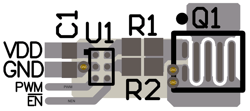
LMG1020 bearcat-layout.gifFigure 15. Typical LMG1020 Layout With Ball-Grid GaN FET And 0402 Decoupling Capacitor
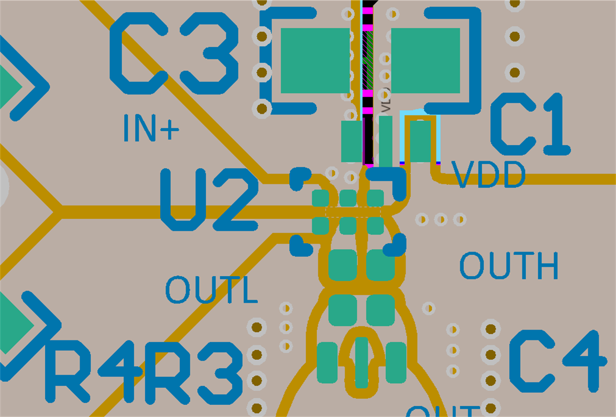
LMG1020 lmg1020-pcb-layout-with-feedthrough-capacitor-snosd45.pngFigure 16. Typical Layout Of LMG1020 And A Feed-Through Decoupling Capacitor With A Capacitor Load