SBOS730A April 2015 – May 2015 LMH6401
PRODUCTION DATA.
- 1 Features
- 2 Applications
- 3 Description
- 4 Revision History
- 5 Device Options
- 6 Pin Configuration and Functions
- 7 Specifications
- 8 Parameter Measurement Information
-
9 Detailed Description
- 9.1 Overview
- 9.2 Functional Block Diagram
- 9.3 Feature Description
- 9.4 Device Functional Modes
- 9.5 Programming
- 9.6
Register Maps
- 9.6.1 Revision ID (address = 0h, Read-Only) [default = 03h]
- 9.6.2 Product ID (address = 1h, Read-Only) [default = 00h]
- 9.6.3 Gain Control (address = 2h) [default = 20h]
- 9.6.4 Reserved (address = 3h) [default = 8Ch]
- 9.6.5 Thermal Feedback Gain Control (address = 4h) [default = 27h]
- 9.6.6 Thermal Feedback Frequency Control (address = 5h) [default = 45h]
- 10Application and Implementation
- 11Power-Supply Recommendations
- 12Layout
- 13Device and Documentation Support
- 14Mechanical, Packaging, and Orderable Information
10 Application and Implementation
NOTE
Information in the following applications sections is not part of the TI component specification, and TI does not warrant its accuracy or completeness. TI’s customers are responsible for determining suitability of components for their purposes. Customers should validate and test their design implementation to confirm system functionality.
10.1 Application Information
10.1.1 Analog Input Characteristics
The LMH6401 is a single-channel device with analog input signal pins (INP and INM) that denote the positive and negative input pins, respectively. The device inputs can be either ac- or dc-coupled. In order to dc-couple the inputs, care must be taken to ensure the common-mode voltage is set within the input common-mode range of the device, as described in the Electrical Characteristics table. For optimal linearity and noise performance, TI recommends setting the input common-mode voltage as close to mid-supply as possible. The LMH6401 device can be ac-coupled at the inputs using input capacitors that allow the inputs to self-bias close to mid-supply and isolates the common-mode voltage of the driving circuitry. The LMH6401 inputs must be driven differentially. For single-ended input source applications, care must be taken to select an appropriate balun or fully-differential amplifier (such as the LMH3401 or LMH5401) that can convert single-ended signals into differential signals with minimal distortion.
At maximum gain, the digital attenuator is set to 0-dB attenuation, the input signal is much smaller than the output, and the maximum output voltage swing is limited by the output stage of the device. At minimum gain, however, the maximum output voltage swing is limited by the input stage because the output is 6 dB lower than the inputs. In the minimum gain configuration, the input signal begins to clip against the electrostatic discharge (ESD) protection diodes before the output reaches maximum swing limits. This clipping is a result of the input signal being unable to swing below the negative supply voltage and being unable to exceed the positive supply voltage because of the protection diodes. For linear operation, care must be taken to ensure that the input is kept within the maximum input voltage ratings, as described in the Absolute Maximum Ratings table. The supply voltage imposes the limit for the input voltage swing because the input stage self-biases to approximately mid-rail.
The device input impedance is set by the internal input termination resistors to a nominal value of 100 Ω. Process variations result in a range of values, as described in the Electrical Characteristics table. The input impedance is also affected by device parasitic reactance at higher frequencies, thus shifting the impedance away from a nominal 100 Ω. The LMH6401 exhibits a well-matched, 100-Ω differential input impedance in the usable bandwidth, achieving a –15-dB input return loss at 2 GHz across the gain settings; see Figure 3. Figure 59 illustrates a Smith chart plot of the LMH6401 differential input impedance referenced to a 100-Ω characteristic impedance.
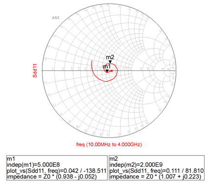 Figure 59. Smith Chart Showing Differential Input Impedance (zO = 100 Ω)
10.1.2 Analog Output Characteristics
The LMH6401, as with most RF amplifiers, has two 10-Ω, on-chip resistors on each output leg to provide isolation from board parasitics at the output pins; see the Functional Block Diagram section. When designing a filter between the LMH6401 and the interfacing circuitry (ADC), the filter source impedance must be calculated by taking into account the two 10-Ω, on-chip resistors. Table 11 shows the calculated external source impedance values (RO+ and RO–) required for various matched filter loads (RL). An important note is that the filter design between the LMH6401 and the ADC is not limited to a matched filter, and source impedance values (RO+ and RO–) can be reduced to achieve higher swing at the filter outputs. Achieving lower loss in the filter source impedance resistors or higher swing at the filter outputs is often desirable because the amplifier must output reduced swing to maintain the same full-scale input at the ADC and, thus, better linearity performance. An example 370-MHz, un-matched, low-pass filter between the LMH6401 and ADS54J60 is illustrated in Figure 64, with (RO+ and RO–) set to 20 Ω and RL set to 100 Ω.
Table 11. Load Component Values(1)
| LOAD (RL) | RO+ AND RO– FOR A MATCHED TERMINATION | TOTAL LOAD RESISTANCE AT AMPLIFIER OUTPUT | TERMINATION LOSS |
|---|---|---|---|
| 50 Ω | 15 Ω | 100 Ω | 6 dB |
| 100 Ω | 40 Ω | 200 Ω | 6 dB |
| 200 Ω | 90 Ω | 400 Ω | 6 dB |
| 400 Ω | 190 Ω | 800 Ω | 6 dB |
| 1 kΩ | 490 Ω | 2000 Ω | 6 dB |
The LMH6401 can be either dc- or ac-coupled at the outputs. For dc-coupled applications, the device provides an option to control the output common-mode voltage using the VOCM pin. Device performance is optimal when the output common-mode voltage is within ±0.5 V of mid-supply (see Figure 21) and performance degrades outside the range when the output swing approaches clipping levels. The LMH6401 can achieve a maximum output swing of 6 VPPD with the output common-mode voltage centered at mid-supply.
Note that by default, the output common-mode voltage is set to mid-supply before the two 10-Ω, on-chip resistors; see the Functional Block Diagram section. On a single-supply operation when dc-coupling the device outputs to an ADC using common-mode, level-shifting resistors, the output common-mode voltage and resistor values being calculated must include the two internal 10-Ω resistors in the equation. When operating the LMH6401 on split supplies and dc-coupling the outputs, TI recommends matching the output common-mode voltage of the LMH6401 with the input common-mode voltage of the ADC. A simple design procedure is to select the supply voltages (VS+ and VS–) such that the default output common-mode voltage being set is equal to the input common-mode voltage of the ADC. As illustrated in Figure 66, the supplies of the LMH6401 are selected such that the default output common-mode voltage is set to mid-supply or 1.23 V, which is within the input common-mode voltage range of the ADC (1.185 V to 1.265 V).
10.1.2.1 Driving Capacitive Loads
With high-speed signal paths, capacitive loading at the output is highly detrimental to the signal path, as shown in Figure 60. The device on-chip resistors are included in order to isolate the parasitic capacitance associated with the package and the printed circuit board (PCB) pads that the device is soldered to. However, designers must make every effort to reduce parasitic loading on the amplifier output pins. The LMH6401 is stable with most capacitive loads up to 10 pF; however, bandwidth suffers with capacitive loading on the output.
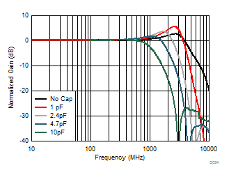 Figure 60. Frequency Response vs Capacitive Load
10.1.3 Thermal Feedback Control
The LMH6401 can be used to optimize long-term settling responses using thermal feedback gain and frequency control registers. These registers are disabled on power-up and can be enabled by clearing the thermal SD bit; see the Thermal Feedback Gain Control register. The thermal feedback gain control bits increase the low-frequency gain and the thermal feedback frequency control bits shift the boost frequency. The thermal feedback gain and frequency registers both have a range of 32 steps. When the function is enabled, there is a small initial gain offset to optimize the control range. The thermal feedback off condition is illustrated in the gain control plot (Figure 61), along with a sweep of gain settings of 0, 4, 8…28, and 31 with a 0 register value representing the minimum gain setting. The frequency control is illustrated in Figure 62 with the optimal gain setting from the gain sweep over the values of 0, 4, 8…28, and 31 with a 0 register value representing the minimum frequency boost setting.
10.1.3.1 Step Response Optimization using Thermal Feedback Control
The LMH6401 has an adjustable frequency compensation scheme that is designed to dramatically improve the step response for long-term settling. The structure of the LMH6401 gives the best distortion performance for signals ranging from dc to 2 GHz over a wide range of gain settings. Thermal heating causes a small change in gain at low frequencies close to 500 kHz. This change in gain is shown in Figure 61 in the ac response for the trace labeled Thermal Feedback OFF. The amount of gain change is approximately 0.18 dB at maximum gain. This gain change resulting from thermal heating leads to approximately 1.7% overshoot that settles over a relatively long time period. A patent pending technique is added that allows for the reduction of this overshoot to approximately 0.35%, thus eliminating the long-term settling and still retaining the wide dynamic performance range. The circuit also corrects for small systematic changes that occur at different gain settings and tracks temperature changes as well. This low-frequency gain correction is accomplished by the addition of a circuit that alters the gain at low frequencies to nearly eliminate the variation from low to high frequencies.
The step response optimization circuit is disabled on power-up and can be enabled by clearing bit 5 in the Thermal Feedback Gain Control register (register 4h). The power-on default setting for thermal gain and frequency are adjusted for the evaluation board for typical silicon performance. These registers are made available for customization in the final system because board layout characteristics or other components in the system can change the required correction needed.
Figure 63 demonstrates the initial step response and the corrected response that corresponds to the default register values for a typical device on the evaluation board displaying long-term settling correction.
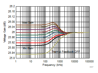 Figure 61. Thermal Gain Control Sweep (Frequency = 9)
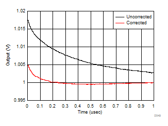 Figure 63. Long-Term Settling Response using Thermal Feedback
 (Gain = 10, Frequency = 9)
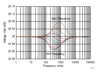 Figure 62. Thermal Frequency Control Sweep (Gain = 10)
10.1.4 Thermal Considerations
The LMH6401 is packaged in a space-saving UQFN package that has a thermal coefficient (RθJA) of 78°C/W. Limit the total power dissipation in order to keep the device junction temperature below 150°C for instantaneous power and below 125°C for continuous power.
10.2 Typical Application
The LMH6401 is designed and optimized for the highest performance when driving differential input ADCs. Figure 64 shows a block diagram of the LMH6401 driving an ADC with a fourth-order, low-pass filter. The primary interface circuit between the amplifier and the ADC is usually an antialiasing filter to suppress high-frequency harmonics aliasing into the ADC FFT spectrum. The interface circuit also provides a means to bias the signal to the input common-mode voltage required by the ADC. Filters range from single-order real RC poles to higher-order RLC filters, depending on the application requirements. Output resistors (RO) in series with the amplifier outputs isolate the amplifier from any capacitive load presented by the filter.
 Figure 64. The LMH6401 Driving an ADS54J60 with a 370 MHz Fourth-Order Chebyshev Low-Pass Filter
Low distortion and low noise figure, along-with low power dissipation make the LMH6401 an ideal device for use in front-end radio applications. Figure 65 shows a block diagram of a one-transmit and one-receive (1T/1R) radio architecture with a digital pre-distortion path, where the LMH6401 can be used as a variable-gain IF amplifier on both the transmit and receive signal chain.
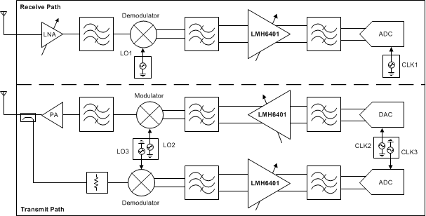 Figure 65. 1T/1R with Digital Pre-Distortion Front-End Radio Application
10.2.1 Design Requirements
Table 12 shows example design requirements for an amplifier in an oscilloscope front-end application; the LMH6401 meets these requirements.
Table 12. Example Design Requirements for an Oscilloscope Front-End application
| SPECIFICATION | DESIGN REQUIREMENTS |
|---|---|
| Supply voltage and current | 4.0 V to 5.25 V with typically less than a 100-mA current and split-supply operation supported |
| Usable input frequency range | DC to 2 GHz |
| Voltage gain and gain range | 26-dB to 10-dB voltage gain with x2 attenuation supported (ideal 32-dB gain range) |
| OIP3 (PO= –2 dBm per tone, RL= 200 Ω) and noise figure (RS = 100 Ω) at 1 GHz | > 30 dBm and less than 10 dB, respectively. |
| Rise and fall time (VO= 2-Vstep) from 10% to 90% | Less than 100 ps |
| Settling time to 1% of VO = 2-Vstep | Less than 1 ns with long-term settling correction required |
10.2.2 Detailed Design Procedure
10.2.2.1 Driving ADCs
When the amplifier is driving an ADC, the key points to consider for implementation are the signal-to-noise ratio (SNR), spurious-free dynamic range (SFDR), and ADC input considerations, as described in this section.
A typical application of the LMH6401 involves driving an ultra-wideband, 12-bit ADC (such as the ADC12J4000), as shown in Figure 66. The LMH6401 can drive the full Nyquist bandwidth of ADCs with sampling rates up to
4 GSPS. If the front-end bandwidth of the ADC is more than 2 GHz, use a simple noise filter to improve SNR. Otherwise, the ADC can be connected directly to the amplifier output pins with appropriate matching resistors to limit the full-scale input of the ADC. Note that the LMH6401 inputs must be driven differentially using a balun or fully-differential amplifiers (FDAs). For dc-coupled applications, an FDA (such as the LMH3401 or LMH5401) that can convert a single-ended input to a differential output with low distortion is preferred.
 Figure 66. DC-Coupled Oscilloscope Front-End Application
10.2.2.1.1 SNR Considerations
The signal-to-noise ratio (SNR) of the amplifier and filter can be calculated from the amplitude of the signal and the bandwidth of the filter. The noise from the amplifier is band-limited by the filter with the equivalent brick-wall filter bandwidth. The amplifier and filter noise can be calculated using Equation 3:

where
- eFILTEROUT = eNAMPOUT • √ENB,
- eNAMPOUT = the output noise density of the LMH6401 (30.4 nV/√Hz) at AV = 26 dB,
- ENB = the brick-wall equivalent noise bandwidth of the filter, and
- VO = the amplifier output signal.
For example, with a first-order (N = 1) band-pass or low-pass filter with a 1000-MHz cutoff, ENB is 1.57 • f–3dB = 1.57 • 1000 MHz = 1570 MHz. For second-order (N = 2) filters, ENB is 1.22 • f–3dB. When the filter order increases, ENB approaches f–3dB (N = 3 → ENB = 1.15 • f–3dB; N = 4 → ENB = 1.13 • f–3dB). Both VO and eFILTEROUT are in RMS voltages. For example, with a 2-VPP (0.707 VRMS) output signal and a 1000-MHz first-order, low-pass filter, the SNR of the amplifier and filter is 55.4 dB with eFILTEROUT = 30.4 nV/√Hz • √1570 MHz = 1204.5 μVRMS.
The SNR of the amplifier, filter, and ADC sum in RMS fashion, as shown in Equation 4 (SNR values in dB):

This formula shows that if the SNR of the amplifier and filter equals the SNR of the ADC, the combined SNR is
3 dB lower (worse). Thus, for minimal degradation (< 1 dB) on the ADC SNR, the SNR of the amplifier and filter must be ≥ 10 dB greater than the ADC SNR. The combined SNR calculated in this manner is usually accurate to within ±1 dB of the actual implementation.
10.2.2.1.2 SFDR Considerations
The SFDR of the amplifier is usually set by the second- or third-harmonic distortion for single-tone inputs, and by the second-order or third-order intermodulation distortion for two-tone inputs. Harmonics and second-order intermodulation distortion can be filtered to some degree, but third-order intermodulation spurs cannot be filtered. The ADC generates the same distortion products as the amplifier, but also generates additional spurs (not harmonically related to the input signal) as a result of sampling and clock feed through.
When the spurs from the amplifier and filter are known, each individual spur can be directly added to the same spur from the ADC, as shown in Equation 5, to estimate the combined spur (spur amplitudes in dBc):

This calculation assumes the spurs are in phase, but usually provides a good estimate of the final combined distortion.
For example, if the spur of the amplifier and filter equals the spur of the ADC, then the combined spur is 6 dB higher. To minimize the amplifier contribution (< 1 dB) to the overall system distortion, the spur from the amplifier and filter must be approximately 15 dB lower in amplitude than that of the converter. The combined spur calculated in this manner is usually accurate to within ±6 dB of the actual implementation; however, higher variations can be detected as a result of phase shift in the filter, especially in second-order harmonic performance.
This worst-case spur calculation assumes that the amplifier and filter spur of interest is in phase with the corresponding spur in the ADC, such that the two spur amplitudes can be added linearly. There are two phase-shift mechanisms that cause the measured distortion performance of the amplifier-ADC chain to deviate from the expected performance calculated using Equation 5; one is the common-mode phase shift and other is the differential phase shift.
Common-mode phase shift is the phase shift detected equally in both branches of the differential signal path including the filter. Common-mode phase shift nullifies the basic assumption that the amplifier, filter, and ADC spur sources are in phase. This phase shift can lead to better performance than predicted when the spurs become phase shifted, and there is the potential for cancellation when the phase shift reaches 180°. However, there is a significant challenge in designing an amplifier-ADC interface circuit to take advantage of a common-mode phase shift for cancellation: the phase characteristics of the ADC spur sources are unknown, thus the necessary phase shift in the filter and signal path for cancellation is also unknown.
Differential phase shift is the difference in the phase response between the two branches of the differential filter signal path. Differential phase shift in the filter is a result of mismatched components caused by nominal tolerances and can severely degrade the even harmonic distortion of the amplifier-ADC chain. This effect has the same result as mismatched path lengths for the two differential traces, and causes more phase shift in one path than the other. Ideally, the phase responses over frequency through the two sides of a differential signal path are identical, such that even harmonics remain optimally out of phase and cancel when the signal is taken differentially. However, if one side has more phase shift than the other, then the even harmonic cancellation is not as effective.
Single-order RC filters cause very little differential phase shift with nominal tolerances of 5% or less, but higher-order LC filters are very sensitive to component mismatch. For instance, a third-order Butterworth band-pass filter with a 100-MHz center frequency and a 20-MHz bandwidth shows as much as 20° of differential phase imbalance in a SPICE Monte Carlo analysis with 2% component tolerances. Therefore, although a prototype may work, production variance is unacceptable. For ac-coupled or dc-coupled applications where a transformer or balun cannot be used, using first- or second-order filters is recommended to minimize the effect of differential phase shift.
10.2.2.1.3 ADC Input Common-Mode Voltage Considerations—AC-Coupled Input
When interfacing to an ADC, the input common-mode voltage range of the ADC must be taken into account for proper operation. In an ac-coupled application between the amplifier and the ADC, the input common-mode voltage bias of the ADC can be accomplished in different ways. Some ADCs use internal bias networks such that the analog inputs are automatically biased to the required input common-mode voltage if the inputs are ac-coupled with capacitors (or if the filter between the amplifier and ADC is a band-pass filter). Other ADCs supply their required input common-mode voltage from a reference voltage output pin (often termed CM or VCM). With these ADCs, the ac-coupled input signal can be re-biased to the input common-mode voltage by connecting resistors from each input to the CM output of the ADC, as shown in Figure 67. AC coupling provides dc common-mode isolation between the amplifier and the ADC; thus, the output common-mode voltage of the amplifier is a don’t care for the ADC.
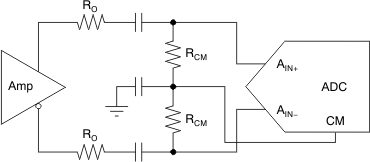 Figure 67. Biasing AC-Coupled ADC Inputs Using the ADC CM Output
10.2.2.1.4 ADC Input Common-Mode Voltage Considerations—DC-Coupled Input
DC-coupled applications vary in complexity and requirements, depending on the ADC (a split supply for the CMV is applicable). One typical requirement is resolving the mismatch between the common-mode voltage of the driving amplifier and the ADC. Devices such as the ADC12J4000 require a nominal 1.23-V input common-mode, whereas other devices such as the ADS54J60 require a nominal 2.1-V input common-mode. The simplest approach when dc-coupling the LMH6401 with the input common-mode voltage of the ADC is to select the supply voltages (VS+) and (VS–) such that the default output common-mode voltage being set is equal to the input common-mode voltage of the ADC; see Figure 66. The default common-mode voltage being set can be controlled externally using the VOCM pin. The device performance is optimal when the output common-mode voltage is within ±0.5 V of mid-supply and degrades outside the range when the output swing approaches clipping levels.
A second approach is shown in Figure 68 when dc-coupling on a single supply, where a resistor network can be used to perform the common-mode level shift. This resistor network consists of the amplifier series output resistors and pullup or pulldown resistors to a reference voltage. This resistor network introduces signal attenuation that may prevent the use of the full-scale input range of the ADC. ADCs with an input common-mode closer to the typical 2.5-V output common-mode of the LMH6401 are easier to dc-couple, and require little or no level shifting.
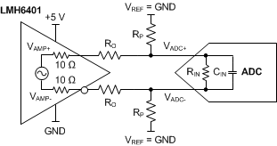 Figure 68. Resistor Network to DC Level-Shift Common-Mode Voltage using VREF as GND
For common-mode analysis of the circuit in Figure 68, assume that VAMP± = VCM and VADC± = VCM (the specification for the ADC input common-mode voltage). Note that the VAMP± common-mode voltage is set before the two internal 10-Ω resistors, making these resistors necessary to include in the common-mode level-shift resistor calculation. VREF is chosen to be a voltage within the system higher than VCM (such as the ADC or amplifier analog supply) or ground, depending on whether the voltage must be pulled up or down, respectively; RO is chosen to be a reasonable value, such as 24.9 Ω. With these known values, RP can be found by using Equation 6:
Shifting the common-mode voltage with the resistor network comes at the expense of signal attenuation. Modeling the ADC input as the parallel combination of a resistance (RIN) and capacitance (CIN) using values taken from the ADC data sheet, the approximate differential input impedance (ZIN) for the ADC can be calculated at the signal frequency. The effect of CIN on the overall calculation of gain is typically minimal and can be ignored for simplicity (that is, ZIN = RIN). The ADC input impedance creates a divider with the resistor network; the gain (attenuation) for this divider can be calculated by Equation 7:
With ADCs that have internal resistors that bias the ADC input to the ADC input common-mode voltage, the effective RIN is equal to twice the value of the bias resistor. For example, the ADS54J60 has a 0.6-kΩ resistor tying each input to the ADC VCM; therefore, the effective differential RIN is 1.2 kΩ.
The introduction of the RP resistors also modifies the effective load that must be driven by the amplifier. Equation 8 shows the effective load created when using the RP resistors.
The RP resistors function in parallel to the ADC input such that the effective load (output current) at the amplifier output is increased. Higher current loads limit the LMH6401 differential output swing.
Using the gain and knowing the full-scale input of the ADC (VADC FS), the required amplitude to drive the ADC with the network can be calculated using Equation 9:

As with any design, testing is recommended to validate whether the specific design goals are met.
10.2.3 Application Curves
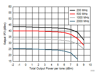 Figure 69. Output IP3 vs Total Output Power per Tone
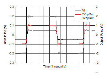 Figure 70. Output Pulse Response
10.3 Do's and Don'ts
10.3.1 Do:
- Include a thermal analysis at the beginning of the project.
- Use well-terminated transmission lines for all signals.
- Maintain symmetrical input and output trace layouts
- Use solid metal layers for the power supplies.
- Keep signal lines as straight as possible.
- Use split supplies where required.
10.3.2 Don't:
- Use a lower supply voltage than necessary.
- Use thin metal traces to supply power.
- Forget about the common-mode response of filters and transmission lines.
- Rout digital line traces close to the analog signals and supply line traces