SBOS730A April 2015 – May 2015 LMH6401
PRODUCTION DATA.
- 1 Features
- 2 Applications
- 3 Description
- 4 Revision History
- 5 Device Options
- 6 Pin Configuration and Functions
- 7 Specifications
- 8 Parameter Measurement Information
-
9 Detailed Description
- 9.1 Overview
- 9.2 Functional Block Diagram
- 9.3 Feature Description
- 9.4 Device Functional Modes
- 9.5 Programming
- 9.6
Register Maps
- 9.6.1 Revision ID (address = 0h, Read-Only) [default = 03h]
- 9.6.2 Product ID (address = 1h, Read-Only) [default = 00h]
- 9.6.3 Gain Control (address = 2h) [default = 20h]
- 9.6.4 Reserved (address = 3h) [default = 8Ch]
- 9.6.5 Thermal Feedback Gain Control (address = 4h) [default = 27h]
- 9.6.6 Thermal Feedback Frequency Control (address = 5h) [default = 45h]
- 10Application and Implementation
- 11Power-Supply Recommendations
- 12Layout
- 13Device and Documentation Support
- 14Mechanical, Packaging, and Orderable Information
8 Parameter Measurement Information
8.1 Setup Diagrams
 Figure 43. Frequency Response Differential Test Setup
 Figure 44. Single-Tone Harmonic Distortion Test Setup
 Figure 45. Two-Tone Linearity Test Setup (OIP3, OIP2)
 Figure 46. Noise Figure Test Setup
8.2 Output Measurement Reference Points
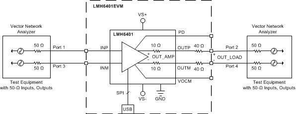
The LMH6401 has two on-chip, 10-Ω output resistors. When matching the output to a 100-Ω load, the evaluation module (EVM) uses an external 40-Ω resistor on each output leg to complete the output matching. Having on-chip output resistors creates two potential reference points for measuring the output voltage. The first reference point is at the internal amplifier output (OUT_AMP), and the second reference point is at the externally-matched 100-Ω load (OUT_LOAD). The measurements in the Electrical Characteristics table and in the Typical Characteristics section are referred to the (OUT_AMP) reference point unless otherwise specified. The conversion between reference points is a straightforward correction of 3 dB for power and 6 dB for voltage, as shown in Equation 1 and Equation 2. The measurements are referenced to OUT_AMP when not specified.
8.3 ATE Testing and DC Measurements
All production testing and dc parameters are measured on automated test equipment capable of dc measurements only. Some measurements (such as voltage gain) are referenced to the output of the internal amplifier and do not include losses attributed to the on-chip output resistors. The Electrical Characteristics values specify these conditions. When the measurement is referred to the amplifier output, the output resistors are not included in the measurement. If the measurement is referred to the device pins, then the output resistor loss is included in the measurement.
8.4 Frequency Response
This test is done by running an S-parameter sweep on a 4-port differential network analyzer using the standard EVM with no baluns; see Figure 43. The inputs and outputs of the EVM are connected to the network analyzer using 50-Ω coaxial cables with all the ports set to a characteristic impedance (ZO) of 50 Ω.
The frequency response test with capacitive load is done by soldering the capacitor across the LMH6401 output pins. In this configuration, the on-chip, 10-Ω resistors on each output leg isolate the capacitive load from the amplifier output pins.
8.5 Distortion
The standard EVM is used for measuring both the single-tone harmonic distortion and two-tone intermodulation distortion; see Figure 44 and Figure 45, respectively. The distortion is measured with differential input signals to the LMH6401. In order to interface with single-ended test equipment, external baluns (1:2, ZO = 50 Ω) are required between the EVM output ports and the test equipment. The Typical Characteristics plots are created with Marki™ baluns, model number BAL-0010. These baluns are used to combine two single tones in the two-tone test plots as well as convert the single-ended input to differential output for harmonic distortion tests. The use of 6-dB attenuator pads on both the inputs and outputs is recommended to provide a balanced match between the external balun and the EVM.
8.6 Noise Figure
This test is done by matching the input of the LMH6401 to a 50-Ω noise source using a 1:2 balun (see Figure 46), with the noise figure being referred to the input impedance (RS = 100 Ω). As noted in Figure 46, an Agilent E4443A with NF features is used for the testing.
8.7 Pulse Response, Slew Rate, and Overdrive Recovery
For time-domain measurements, the standard EVM is driven through a balun again to convert a single-ended output from the test equipment to the differential inputs of the LMH6401. The differential outputs are directly connected to the oscilloscope inputs, with the differential signal response calculated using trace math from the two separate oscilloscope inputs.
8.8 Power Down
The standard EVM is used for this test by completely removing the shorting block on jumper JPD. A high-speed, 50-Ω pulse generator is used to drive the PD pin, which toggles the output signal on or off depending upon the PD pin voltage.
8.9 VOCM Frequency Response
The standard EVM is used for this test. A network analyzer is connected to the VOCM input of the EVM and the EVM outputs are connected to the network analyzer with 50-Ω coaxial cables. The network analyzer analysis mode is set to single-ended input and differential output, and the output common-mode response is measured with respect to the single-ended input (Scs21). The input signal frequency is swept with the signal level set for 100 mV (–16 dBm). Note that the common-mode control circuit gain is approximately one.