SNAS489K March 2011 – December 2014 LMK04803 , LMK04805 , LMK04806 , LMK04808
PRODUCTION DATA.
- 1 Features
- 2 Applications
- 3 Description
- 4 Revision History
- 5 Pin Configuration and Functions
- 6 Specifications
-
7 Parameter Measurement Information
- 7.1
Charge Pump Current Specification Definitions
- 7.1.1 Charge Pump Output Current Magnitude Variation Vs. Charge Pump Output Voltage
- 7.1.2 Charge Pump Sink Current Vs. Charge Pump Output Source Current Mismatch
- 7.1.3 Charge Pump Output Current Magnitude Variation vs. Ambient Temperature"Temperature" to "Ambient Temperature" in heading titled "Charge Pump Output Current Magnitude Variation vs. Ambient Temperature"
- 7.2 Differential Voltage Measurement Terminology
- 7.1
Charge Pump Current Specification Definitions
-
8 Detailed Description
- 8.1
Overview
- 8.1.1 System Architecture
- 8.1.2 PLL1 Redundant Reference Inputs (CLKin0/CLKin0* and CLKin1/CLKin1*)
- 8.1.3 PLL1 Tunable Crystal Support
- 8.1.4 VCXO/CRYSTAL Buffered Outputs
- 8.1.5 Frequency Holdover
- 8.1.6 Integrated Loop Filter Poles
- 8.1.7 Internal VCO
- 8.1.8 External VCO Mode
- 8.1.9 Clock Distribution
- 8.1.10 0-Delay
- 8.1.11 Default Startup Clocks
- 8.1.12 Status Pins
- 8.1.13 Register Readback
- 8.2 Functional Block Diagram
- 8.3
Feature Description
- 8.3.1 Serial MICROWIRE Timing Diagram
- 8.3.2 Advanced MICROWIRE Timing Diagrams
- 8.3.3 Inputs / Outputs
- 8.3.4 Input Clock Switching
- 8.3.5 Holdover Mode
- 8.3.6 PLLs
- 8.3.7 Status Pins
- 8.3.8 VCO
- 8.3.9
Clock Distribution
- 8.3.9.1 Fixed Digital Delay
- 8.3.9.2 Fixed Digital Delay - Example
- 8.3.9.3
Clock Output Synchronization (SYNC)
- 8.3.9.3.1 Effect of SYNC
- 8.3.9.3.2 Methods of Generating SYNC
- 8.3.9.3.3 Avoiding Clock Output Interruption Due to Sync
- 8.3.9.3.4 SYNC Timing
- 8.3.9.3.5
Dynamically Programming Digital Delay
- 8.3.9.3.5.1 Absolute vs. Relative Dynamic Digital Delay
- 8.3.9.3.5.2 Dynamic Digital Delay and 0-Delay Mode
- 8.3.9.3.5.3 SYNC and Minimum Step Size
- 8.3.9.3.5.4 Programming Overview
- 8.3.9.3.5.5 Internal Dynamic Digital Delay Timing
- 8.3.9.3.5.6 Other Timing Requirements
- 8.3.9.3.5.7 Absolute Dynamic Digital Delay
- 8.3.9.3.5.8 Relative Dynamic Digital Delay
- 8.3.10 0-Delay Mode
- 8.4 Device Functional Modes
- 8.5 Programming
- 8.6
Register Maps
- 8.6.1 Register Map and Readback Register Map
- 8.6.2 Default Device Register Settings After Power On Reset
- 8.6.3
Register Descriptions
- 8.6.3.1
Register R0 TO R5
- 8.6.3.1.1 CLKoutX_Y_PD, Powerdown CLKoutX_Y Output Path
- 8.6.3.1.2 CLKoutX_Y_OSCin_Sel, Clock Group Source
- 8.6.3.1.3 CLKoutY_ADLY_SEL[29], CLKoutX_ADLY_SEL[28], Select Analog Delay
- 8.6.3.1.4 CLKoutX_Y_DDLY, Clock Channel Digital Delay
- 8.6.3.1.5 Reset
- 8.6.3.1.6 POWERDOWN
- 8.6.3.1.7 CLKoutX_Y_HS, Digital Delay Half Shift
- 8.6.3.1.8 CLKoutX_Y_DIV, Clock Output Divide
- 8.6.3.2 Registers R6 TO R8
- 8.6.3.3
Register R10
- 8.6.3.3.1 OSCout1_LVPECL_AMP, LVPECL Output Amplitude Control
- 8.6.3.3.2 OSCout0_TYPE
- 8.6.3.3.3 EN_OSCoutX, OSCout Output Enable
- 8.6.3.3.4 OSCoutX_MUX, Clock Output Mux
- 8.6.3.3.5 PD_OSCin, OSCin Powerdown Control
- 8.6.3.3.6 OSCout_DIV, Oscillator Output Divide
- 8.6.3.3.7 VCO_MUX
- 8.6.3.3.8 EN_FEEDBACK_MUX
- 8.6.3.3.9 VCO_DIV, VCO Divider
- 8.6.3.3.10 FEEDBACK_MUX
- 8.6.3.4 Register R11
- 8.6.3.5 Register R12
- 8.6.3.6 Register R13
- 8.6.3.7 Register 14
- 8.6.3.8 REGISTER 15
- 8.6.3.9 Register 16
- 8.6.3.10 Register 23
- 8.6.3.11
Register 24
- 8.6.3.11.1 PLL2_C4_LF, PLL2 Integrated Loop Filter Component
- 8.6.3.11.2 PLL2_C3_LF, PLL2 Integrated Loop Filter Component
- 8.6.3.11.3 PLL2_R4_LF, PLL2 Integrated Loop Filter Component
- 8.6.3.11.4 PLL2_R3_LF, PLL2 Integrated Loop Filter Component
- 8.6.3.11.5 PLL1_N_DLY
- 8.6.3.11.6 PLL1_R_DLY
- 8.6.3.11.7 PLL1_WND_SIZE
- 8.6.3.12 Register 25
- 8.6.3.13 Register 26
- 8.6.3.14 REGISTER 27
- 8.6.3.15 Register 28
- 8.6.3.16 Register 29
- 8.6.3.17 Register 30
- 8.6.3.18 Register 31
- 8.6.3.1
Register R0 TO R5
- 8.1
Overview
-
9 Application and Implementation
- 9.1
Application Information
- 9.1.1 Loop Filter
- 9.1.2 Driving CLKin and OSCin Inputs
- 9.1.3 Termination and Use of Clock Output (Drivers)
- 9.1.4 Frequency Planning with the LMK0480x Family
- 9.1.5 PLL Programming
- 9.1.6 Digital Lock Detect Frequency Accuracy
- 9.1.7 Calculating Dynamic Digital Delay Values for any Divide
- 9.1.8 Optional Crystal Oscillator Implementation (OSCin/OSCin*)
- 9.1.9 Application Curves
- 9.2 Typical Applications
- 9.3 System Examples
- 9.4 Do's and Don'ts
- 9.1
Application Information
- 10Power Supply Recommendations
- 11Layout
- 12Device and Documentation Support
- 13Mechanical, Packaging, and Orderable Information
パッケージ・オプション
メカニカル・データ(パッケージ|ピン)
- NKD|64
サーマルパッド・メカニカル・データ
- NKD|64
発注情報
5 Pin Configuration and Functions
64-Pin WQFN with Exposed Pad
NKD Package
(Top View)
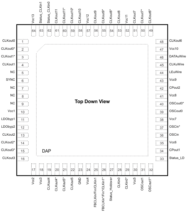
Pin Functions(1)
| PIN | I/O | TYPE | DESCRIPTION | |
|---|---|---|---|---|
| NUMBER | NAME | |||
| 1, 2 | CLKout0, CLKout0* | O | Programmable | Clock output 0 (clock group 0). |
| 3, 4 | CLKout1*, CLKout1 | O | Programmable | Clock output 1 (clock group 0). |
| 6 | SYNC | I/O | Programmable | CLKout Synchronization input or programmable status pin. |
| 5, 7, 8, 9 | NC | – | – | No Connection. These pins must be left floating. |
| 10 | Vcc1 | PWR | Power supply for VCO LDO. | |
| 11 | LDObyp1 | ANLG | LDO Bypass, bypassed to ground with 10 µF capacitor. | |
| 12 | LDObyp2 | ANLG | LDO Bypass, bypassed to ground with a 0.1 µF capacitor. | |
| 13, 14 | CLKout2, CLKout2* | O | Programmable | Clock output 2 (clock group 1). |
| 15, 16 | CLKout3*, CLKout3 | O | Programmable | Clock output 3 (clock group 1). |
| 17 | Vcc2 | PWR | Power supply for clock group 1: CLKout2 and CLKout3. | |
| 18 | Vcc3 | PWR | Power supply for clock group 2: CLKout4 and CLKout5. | |
| 19, 20 | CLKout4, CLKout4* | O | Programmable | Clock output 4 (clock group 2). |
| 21, 22 | CLKout5*, CLKout5 | O | Programmable | Clock output 5 (clock group 2). |
| 23 | GND | PWR | Ground. | |
| 24 | Vcc4 | PWR | Power supply for digital. | |
| 25, 26 | CLKin1, CLKin1* | I | ANLG | Reference Clock Input Port 1 for PLL1. AC or DC Coupled. |
| FBCLKin, FBCLKin* | Feedback input for external clock feedback input (0-delay mode). AC or DC Coupled. | |||
| Fin/Fin* | External VCO input (External VCO mode). AC or DC Coupled. | |||
| 27 | Status_Holdover | I/O | Programmable | Programmable status pin, default readback output. Programmable to holdover mode indicator. Other options available by programming. |
| 28, 29 | CLKin0, CLKin0* | I | ANLG | Reference Clock Input Port 0 for PLL1. AC or DC Coupled. |
| 30 | Vcc5 | PWR | Power supply for clock inputs and OSCout1. | |
| 31, 32 | OSCout1, OSCout1* | O | LVPECL | Buffered output 1 of OSCin port. |
| 33 | Status_LD | I/O | Programmable | Programmable status pin, default lock detect for PLL1 and PLL2. Other options available by programming. |
| 34 | CPout1 | O | ANLG | Charge pump 1 output. |
| 35 | Vcc6 | PWR | Power supply for PLL1, charge pump 1. | |
| 36, 37 | OSCin, OSCin* | I | ANLG | Feedback to PLL1, Reference input to PLL2. AC Coupled. |
| 38 | Vcc7 | PWR | Power supply for OSCin, OSCout0, and PLL2 circuitry.(2) | |
| 39, 40 | OSCout0, OSCout0* | O | Programmable | Buffered output 0 of OSCin port.(2) |
| 41 | Vcc8 | PWR | Power supply for PLL2, charge pump 2. | |
| 42 | CPout2 | O | ANLG | Charge pump 2 output. |
| 43 | Vcc9 | PWR | Power supply for PLL2. | |
| 44 | LEuWire | I | CMOS | MICROWIRE Latch Enable Input. |
| 45 | CLKuWire | I | CMOS | MICROWIRE Clock Input. |
| 46 | DATAuWire | I | CMOS | MICROWIRE Data Input. |
| 47 | Vcc10 | PWR | Power supply for clock group 3: CLKout6 and CLKout7. | |
| 48, 49 | CLKout6, CLKout6* | O | Programmable | Clock output 6 (clock group 3). |
| 50, 51 | CLKout7*, CLKout7 | O | Programmable | Clock output 7 (clock group 3). |
| 52 | Vcc11 | PWR | Power supply for clock group 4: CLKout8 and CLKout9. | |
| 53, 54 | CLKout8, CLKout8* | O | Programmable | Clock output 8 (clock group 4). |
| 55, 56 | CLKout9*, CLKout9 | O | Programmable | Clock output 9 (clock group 4). |
| 57 | Vcc12 | PWR | Power supply for clock group 5: CLKout10 and CLKout11. | |
| 58, 59 | CLKout10, CLKout10* | O | Programmable | Clock output 10 (clock group 5). |
| 60, 61 | CLKout11*, CLKout11 | O | Programmable | Clock output 11 (clock group 5). |
| 62 | Status_CLKin0 | I/O | Programmable | Programmable status pin. Default is input for pin control of PLL1 reference clock selection. CLKin0 LOS status and other options available by programming. |
| 63 | Status_CLKin1 | I/O | Programmable | Programmable status pin. Default is input for pin control of PLL1 reference clock selection. CLKin1 LOS status and other options available by programming. |
| 64 | Vcc13 | PWR | Power supply for clock group 0: CLKout0 and CLKout1. | |
| DAP | DAP | – | GND | DIE ATTACH PAD, connect to GND. |
(1) See Pin Connection Recommendations.
(2) See Vcc5 (CLKin and OSCout1), Vcc7 (OSCin and OSCout0) for information on configuring device for optimum performance.