SNAS489K March 2011 – December 2014 LMK04803 , LMK04805 , LMK04806 , LMK04808
PRODUCTION DATA.
- 1 Features
- 2 Applications
- 3 Description
- 4 Revision History
- 5 Pin Configuration and Functions
- 6 Specifications
-
7 Parameter Measurement Information
- 7.1
Charge Pump Current Specification Definitions
- 7.1.1 Charge Pump Output Current Magnitude Variation Vs. Charge Pump Output Voltage
- 7.1.2 Charge Pump Sink Current Vs. Charge Pump Output Source Current Mismatch
- 7.1.3 Charge Pump Output Current Magnitude Variation vs. Ambient Temperature"Temperature" to "Ambient Temperature" in heading titled "Charge Pump Output Current Magnitude Variation vs. Ambient Temperature"
- 7.2 Differential Voltage Measurement Terminology
- 7.1
Charge Pump Current Specification Definitions
-
8 Detailed Description
- 8.1
Overview
- 8.1.1 System Architecture
- 8.1.2 PLL1 Redundant Reference Inputs (CLKin0/CLKin0* and CLKin1/CLKin1*)
- 8.1.3 PLL1 Tunable Crystal Support
- 8.1.4 VCXO/CRYSTAL Buffered Outputs
- 8.1.5 Frequency Holdover
- 8.1.6 Integrated Loop Filter Poles
- 8.1.7 Internal VCO
- 8.1.8 External VCO Mode
- 8.1.9 Clock Distribution
- 8.1.10 0-Delay
- 8.1.11 Default Startup Clocks
- 8.1.12 Status Pins
- 8.1.13 Register Readback
- 8.2 Functional Block Diagram
- 8.3
Feature Description
- 8.3.1 Serial MICROWIRE Timing Diagram
- 8.3.2 Advanced MICROWIRE Timing Diagrams
- 8.3.3 Inputs / Outputs
- 8.3.4 Input Clock Switching
- 8.3.5 Holdover Mode
- 8.3.6 PLLs
- 8.3.7 Status Pins
- 8.3.8 VCO
- 8.3.9
Clock Distribution
- 8.3.9.1 Fixed Digital Delay
- 8.3.9.2 Fixed Digital Delay - Example
- 8.3.9.3
Clock Output Synchronization (SYNC)
- 8.3.9.3.1 Effect of SYNC
- 8.3.9.3.2 Methods of Generating SYNC
- 8.3.9.3.3 Avoiding Clock Output Interruption Due to Sync
- 8.3.9.3.4 SYNC Timing
- 8.3.9.3.5
Dynamically Programming Digital Delay
- 8.3.9.3.5.1 Absolute vs. Relative Dynamic Digital Delay
- 8.3.9.3.5.2 Dynamic Digital Delay and 0-Delay Mode
- 8.3.9.3.5.3 SYNC and Minimum Step Size
- 8.3.9.3.5.4 Programming Overview
- 8.3.9.3.5.5 Internal Dynamic Digital Delay Timing
- 8.3.9.3.5.6 Other Timing Requirements
- 8.3.9.3.5.7 Absolute Dynamic Digital Delay
- 8.3.9.3.5.8 Relative Dynamic Digital Delay
- 8.3.10 0-Delay Mode
- 8.4 Device Functional Modes
- 8.5 Programming
- 8.6
Register Maps
- 8.6.1 Register Map and Readback Register Map
- 8.6.2 Default Device Register Settings After Power On Reset
- 8.6.3
Register Descriptions
- 8.6.3.1
Register R0 TO R5
- 8.6.3.1.1 CLKoutX_Y_PD, Powerdown CLKoutX_Y Output Path
- 8.6.3.1.2 CLKoutX_Y_OSCin_Sel, Clock Group Source
- 8.6.3.1.3 CLKoutY_ADLY_SEL[29], CLKoutX_ADLY_SEL[28], Select Analog Delay
- 8.6.3.1.4 CLKoutX_Y_DDLY, Clock Channel Digital Delay
- 8.6.3.1.5 Reset
- 8.6.3.1.6 POWERDOWN
- 8.6.3.1.7 CLKoutX_Y_HS, Digital Delay Half Shift
- 8.6.3.1.8 CLKoutX_Y_DIV, Clock Output Divide
- 8.6.3.2 Registers R6 TO R8
- 8.6.3.3
Register R10
- 8.6.3.3.1 OSCout1_LVPECL_AMP, LVPECL Output Amplitude Control
- 8.6.3.3.2 OSCout0_TYPE
- 8.6.3.3.3 EN_OSCoutX, OSCout Output Enable
- 8.6.3.3.4 OSCoutX_MUX, Clock Output Mux
- 8.6.3.3.5 PD_OSCin, OSCin Powerdown Control
- 8.6.3.3.6 OSCout_DIV, Oscillator Output Divide
- 8.6.3.3.7 VCO_MUX
- 8.6.3.3.8 EN_FEEDBACK_MUX
- 8.6.3.3.9 VCO_DIV, VCO Divider
- 8.6.3.3.10 FEEDBACK_MUX
- 8.6.3.4 Register R11
- 8.6.3.5 Register R12
- 8.6.3.6 Register R13
- 8.6.3.7 Register 14
- 8.6.3.8 REGISTER 15
- 8.6.3.9 Register 16
- 8.6.3.10 Register 23
- 8.6.3.11
Register 24
- 8.6.3.11.1 PLL2_C4_LF, PLL2 Integrated Loop Filter Component
- 8.6.3.11.2 PLL2_C3_LF, PLL2 Integrated Loop Filter Component
- 8.6.3.11.3 PLL2_R4_LF, PLL2 Integrated Loop Filter Component
- 8.6.3.11.4 PLL2_R3_LF, PLL2 Integrated Loop Filter Component
- 8.6.3.11.5 PLL1_N_DLY
- 8.6.3.11.6 PLL1_R_DLY
- 8.6.3.11.7 PLL1_WND_SIZE
- 8.6.3.12 Register 25
- 8.6.3.13 Register 26
- 8.6.3.14 REGISTER 27
- 8.6.3.15 Register 28
- 8.6.3.16 Register 29
- 8.6.3.17 Register 30
- 8.6.3.18 Register 31
- 8.6.3.1
Register R0 TO R5
- 8.1
Overview
-
9 Application and Implementation
- 9.1
Application Information
- 9.1.1 Loop Filter
- 9.1.2 Driving CLKin and OSCin Inputs
- 9.1.3 Termination and Use of Clock Output (Drivers)
- 9.1.4 Frequency Planning with the LMK0480x Family
- 9.1.5 PLL Programming
- 9.1.6 Digital Lock Detect Frequency Accuracy
- 9.1.7 Calculating Dynamic Digital Delay Values for any Divide
- 9.1.8 Optional Crystal Oscillator Implementation (OSCin/OSCin*)
- 9.1.9 Application Curves
- 9.2 Typical Applications
- 9.3 System Examples
- 9.4 Do's and Don'ts
- 9.1
Application Information
- 10Power Supply Recommendations
- 11Layout
- 12Device and Documentation Support
- 13Mechanical, Packaging, and Orderable Information
パッケージ・オプション
メカニカル・データ(パッケージ|ピン)
- NKD|64
サーマルパッド・メカニカル・データ
- NKD|64
発注情報
6 Specifications
6.1 Absolute Maximum Ratings(1)(2)(4)
over operating free-air temperature range (unless otherwise noted) (5)| MIN | MAX | UNIT | ||
|---|---|---|---|---|
| VCC | Supply Voltage (3) | –0.3 | 3.6 | V |
| VIN | Input Voltage | –0.3 | (VCC + 0.3) | V |
| TL | Lead Temperature (solder 4 seconds) | +260 | °C | |
| TJ | Junction Temperature | 150 | °C | |
| IIN | Differential Input Current (CLKinX/X*, OSCin/OSCin*, FBCLKin/FBCLKin*, Fin/Fin*) |
± 5 | mA | |
| MSL | Moisture Sensitivity Level | 3 | ||
| Tstg | Storage temperature range | -65 | 150 | °C |
(1) "Absolute Maximum Ratings" indicate limits beyond which damage to the device may occur. Operating Ratings indicate conditions for which the device is intended to be functional, but do not ensure specific performance limits. For ensured specifications and test conditions, see the Electrical Characteristics. The ensured specifications apply only to the test conditions listed.
(2) Stresses in excess of the absolute maximum ratings can cause permanent or latent damage to the device. These are absolute stress ratings only. Functional operation of the device is only implied at these or any other conditions in excess of those given in the operation sections of the data sheet. Exposure to absolute maximum ratings for extended periods can adversely affect device reliability.
(3) Never to exceed 3.6 V.
(4) If Military/Aerospace specified devices are required, contact the Texas Instruments Sales Office/Distributors for availability and specifications.
(5) Stresses beyond those listed under Absolute Maximum Ratings may cause permanent damage to the device. These are stress ratings only, which do not imply functional operation of the device at these or any other conditions beyond those indicated under Recommended Operating Conditions. Exposure to absolute-maximum-rated conditions for extended periods may affect device reliability.
6.2 ESD Ratings
| VALUE | UNIT | |||
|---|---|---|---|---|
| V(ESD) | Electrostatic discharge | Human-body model (HBM), per ANSI/ESDA/JEDEC JS-001(1) | ±2000 | V |
| Machine model (MM) | ±150 | |||
| Charged-device model (CDM), per JEDEC specification JESD22-C101(2) | ±750 | |||
(1) JEDEC document JEP155 states that 500-V HBM allows safe manufacturing with a standard ESD control process. Manufacturing with less than 500-V HBM is possible with the necessary precautions. Pins listed as ±2000 V may actually have higher performance.
(2) JEDEC document JEP157 states that 250-V CDM allows safe manufacturing with a standard ESD control process. Manufacturing with less than 250-V CDM is possible with the necessary precautions. Pins listed as ±750 V may actually have higher performance.
6.3 Recommended Operating Conditions
| MIN | NOM | MAX | UNIT | |||
|---|---|---|---|---|---|---|
| TJ | Junction Temperature | 125 | °C | |||
| TA | Ambient Temperature | VCC = 3.3 V | -40 | 25 | 85 | °C |
| VCC | Supply Voltage | 3.15 | 3.3 | 3.45 | V |
6.4 Thermal Information
| THERMAL METRIC(1) | LMK0480x | UNIT | |
|---|---|---|---|
| NKD | |||
| 64 PINS | |||
| RθJA | Junction-to-ambient thermal resistance on 4-layer JEDEC PCB(2)(8) | 25.2 | °C/W |
| RθJC(top) | Junction-to-case (top) thermal resistance(3)(9) | 6.9 | |
| RθJB | Junction-to-board thermal resistance(4) | 4.0 | |
| ψJT | Junction-to-top characterization parameter(5) | 0.1 | |
| ψJB | Junction-to-board characterization parameter(6) | 4.0 | |
| RθJC(bot) | Junction-to-case (bottom) thermal resistance(7) | 0.8 | |
(1) For more information about traditional and new thermal metrics, see the IC Package Thermal Metrics application report, SPRA953.
(2) The junction-to-ambient thermal resistance under natural convection is obtained in a simulation on a JEDEC-standard, High-K board, as specified in JESD51-7, in an environment described in JESD51-2a.
(3) The junction-to-case(top) thermal resistance is obtained by simulating a cold plate test on the package top. No specific JEDEC standard test exists, but a close description can be found in the ANSI SEMI standard G30-88.
(4) The junction-to-board thermal resistance is obtained by simulating an environment with a ring cold plate fixture to control the PCB temperature, as described in JESD51-8.
(5) The junction-to-top characterization parameter, ψJT, estimates the junction temperature of a device in a real system and is extracted from the simulation data for obtaining RθJA, using a procedure described in JESD51-2a (sections 6 and 7).
(6) The junction-to-board characterization parameter, ψJB, estimates the junction temperature of a device in a real system and is extracted from the simulation data for obtaining RθJA, using a procedure described in JESD51-2a (sections 6 and 7).
(7) The junction-to-case(bottom) thermal resistance is obtained by simulating a cold plate test on the exposed (power) pad. No specific JEDEC standard test exists, but a close description can be found in the ANSI SEMI standard G30-88.
(8) Specification assumes 32 thermal vias connect the die attach pad to the embedded copper plane on the 4-layer JEDEC PCB. These vias play a key role in improving the thermal performance of the WQFN. Note that the JEDEC PCB is a standard thermal measurement PCB and does not represent best performance a PCB can achieve. It is recommended that the maximum number of vias be used in the board layout. R θJA is unique for each PCB.
(9) Case is defined as the DAP (die attach pad)
6.5 Electrical Characteristics
3.15 V ≤ VCC ≤ 3.45 V, -40 °C ≤ TA ≤ 85°C. Typical values represent most likely parametric norms at VCC = 3.3 V, TA = 25°C, at the Recommended Operating Conditions at the time of product characterization and are not specified.(5)| PARAMETER | TEST CONDITIONS | MIN | TYP | MAX | UNIT | |
|---|---|---|---|---|---|---|
| CURRENT CONSUMPTION | ||||||
| ICC_PD | Power down supply current | No DC path to ground on OSCout1/1*(1) | 1 | 3 | mA | |
| ICC_CLKS | Supply current with all clocks enabled(3) | All clock delays disabled, CLKoutX_Y_DIV = 1045, CLKoutX_TYPE = 1 (LVDS), PLL1 and PLL2 locked. |
505 | 590 | mA | |
| CLKin0/0* and CLKin1/1* INPUT CLOCK SPECIFICATIONS | ||||||
| fCLKin | Clock input frequency(4) | 0.001 | 500 | MHz | ||
| SLEWCLKin(5) | Clock input slew rate(18) | 20% to 80% | 0.15 | 0.5 | V/ns | |
| VIDCLKin | Clock input Differential input voltage (see (2) and Figure 4) |
AC coupled CLKinX_BUF_TYPE = 0 (Bipolar) |
0.25 | 1.55 | |V| | |
| VSSCLKin | 0.5 | 3.1 | Vpp | |||
| VIDCLKin | AC coupled CLKinX_BUF_TYPE = 1 (MOS) |
0.25 | 1.55 | |V| | ||
| VSSCLKin | 0.5 | 3.1 | Vpp | |||
| VCLKin | Clock input Single-ended input voltage(18) |
AC coupled to CLKinX; CLKinX* AC coupled to Ground CLKinX_BUF_TYPE = 0 (Bipolar) |
0.25 | 2.4 | Vpp | |
| AC coupled to CLKinX; CLKinX* AC coupled to Ground CLKinX_BUF_TYPE = 1 (MOS) |
0.25 | 2.4 | Vpp | |||
| VCLKin0-offset | DC offset voltage between CLKin0/CLKin0* CLKin0* - CLKin0 |
Each pin AC coupled CLKin0_BUF_TYPE = 0 (Bipolar) |
20 | mV | ||
| VCLKin1-offset | DC offset voltage between CLKin1/CLKin1* CLKin1* - CLKin1 |
0 | mV | |||
| VCLKinX-offset | DC offset voltage between CLKinX/CLKinX* CLKinX* - CLKinX |
Each pin AC coupled CLKinX_BUF_TYPE = 1 (MOS) |
55 | mV | ||
| VCLKin- VIH | High input voltage | DC coupled to CLKinX; CLKinX* AC coupled to Ground CLKinX_BUF_TYPE = 1 (MOS) |
2.0 | VCC | V | |
| VCLKin- VIL | Low input voltage | 0.0 | 0.4 | V | ||
| FBCLKin/FBCLKin* and Fin/Fin* INPUT SPECIFICATIONS | ||||||
| fFBCLKin | Clock input frequency(18) | AC coupled (CLKinX_BUF_TYPE = 0) MODE = 2 or 8; FEEDBACK_MUX = 6 |
0.001 | 1000 | MHz | |
| fFin | Clock input frequency(18) | AC coupled (CLKinX_BUF_TYPE = 0) MODE = 3 or 11 |
0.001 | 3100 | MHz | |
| VFBCLKin/Fin | Single Ended Clock input voltage(18) |
AC coupled; (CLKinX_BUF_TYPE = 0) |
0.25 | 2.0 | Vpp | |
| SLEWFBCLKin/Fin | Slew rate on CLKin(18) | AC coupled; 20% to 80%; (CLKinX_BUF_TYPE = 0) |
0.15 | 0.5 | V/ns | |
| PLL1 SPECIFICATIONS | ||||||
| fPD1 | PLL1 phase detector frequency | 40 | MHz | |||
| ICPout1SOURCE | PLL1 charge Pump source current(6) |
VCPout1 = VCC/2, PLL1_CP_GAIN = 0 | 100 | µA | ||
| VCPout1 = VCC/2, PLL1_CP_GAIN = 1 | 200 | |||||
| VCPout1 = VCC/2, PLL1_CP_GAIN = 2 | 400 | |||||
| VCPout1 = VCC/2, PLL1_CP_GAIN = 3 | 1600 | |||||
| ICPout1SINK | PLL1 charge Pump sink current(6) |
VCPout1=VCC/2, PLL1_CP_GAIN = 0 | -100 | µA | ||
| VCPout1=VCC/2, PLL1_CP_GAIN = 1 | -200 | |||||
| VCPout1=VCC/2, PLL1_CP_GAIN = 2 | -400 | |||||
| VCPout1=VCC/2, PLL1_CP_GAIN = 3 | -1600 | |||||
| ICPout1%MIS | Charge pump Sink/source mismatch |
VCPout1 = VCC/2, T = 25 °C | 3% | 10% | ||
| ICPout1VTUNE | Magnitude of charge pump current variation vs. charge pump voltage | 0.5 V < VCPout1 < VCC - 0.5 V TA = 25 °C |
4% | |||
| ICPout1%TEMP | Charge pump current vs. temperature variation |
4% | ||||
| ICPout1 TRI | Charge Pump TRI-STATE leakage current | 0.5 V < VCPout < VCC - 0.5 V | 5 | nA | ||
| PN10kHz | PLL 1/f noise at 10 kHz offset.(10) Normalized to 1 GHz Output Frequency | PLL1_CP_GAIN = 400 µA | -117 | dBc/Hz | ||
| PLL1_CP_GAIN = 1600 µA | -118 | |||||
| PN1Hz | Normalized phase noise contribution(11) | PLL1_CP_GAIN = 400 µA | -221.5 | dBc/Hz | ||
| PLL1_CP_GAIN = 1600 µA | -223 | |||||
| PLL2 REFERENCE INPUT (OSCin) SPECIFICATIONS | ||||||
| fOSCin | PLL2 reference input(7) | 500 | MHz | |||
| SLEWOSCin | PLL2 reference clock minimum slew rate on OSCin(18) | 20% to 80% | 0.15 | 0.5 | V/ns | |
| VOSCin | Input voltage for OSCin or OSCin*(18) | AC coupled; Single-ended (Unused pin AC coupled to GND) | 0.2 | 2.4 | Vpp | |
| VIDOSCin | Differential voltage swing (see Figure 4) | AC coupled | 0.2 | 1.55 | |V| | |
| VSSOSCin | 0.4 | 3.1 | Vpp | |||
| VOSCin-offset | DC offset voltage between OSCin/OSCin* OSCinX* - OSCinX |
Each pin AC coupled | 20 | mV | ||
| fdoubler_max | Doubler input frequency(18) | EN_PLL2_REF_2X = 1;(8)
OSCin Duty Cycle 40% to 60% |
155 | MHz | ||
| CRYSTAL OSCILLATOR MODE SPECIFICATIONS | ||||||
| fXTAL | Crystal frequency range(18) | RESR < 40 Ω | 6 | 20.5 | MHz | |
| PXTAL | Crystal power dissipation(9) | Vectron VXB1 crystal, 20.48 MHz, RESR < 40 Ω XTAL_LVL = 0 |
100 | µW | ||
| CIN | Input capacitance of LMK0480x OSCin port |
-40 to +85 °C | 6 | pF | ||
| PLL2 PHASE DETECTOR and CHARGE PUMP SPECIFICATIONS | ||||||
| fPD2 | Phase detector frequency | 155 | MHz | |||
| ICPoutSOURCE | PLL2 charge pump source current(6) | VCPout2=VCC/2, PLL2_CP_GAIN = 0 | 100 | µA | ||
| VCPout2=VCC/2, PLL2_CP_GAIN = 1 | 400 | |||||
| VCPout2=VCC/2, PLL2_CP_GAIN = 2 | 1600 | |||||
| VCPout2=VCC/2, PLL2_CP_GAIN = 3 | 3200 | |||||
| ICPoutSINK | PLL2 charge pump sink current(6) | VCPout2=VCC/2, PLL2_CP_GAIN = 0 | -100 | µA | ||
| VCPout2=VCC/2, PLL2_CP_GAIN = 1 | -400 | |||||
| VCPout2=VCC/2, PLL2_CP_GAIN = 2 | -1600 | |||||
| VCPout2=VCC/2, PLL2_CP_GAIN = 3 | -3200 | |||||
| ICPout2%MIS | Charge pump sink/source mismatch | VCPout2=VCC/2, TA = 25 °C | 3% | 10% | ||
| ICPout2VTUNE | Magnitude of charge pump current vs. charge pump voltage variation | 0.5 V < VCPout2 < VCC - 0.5 V TA = 25 °C |
4% | |||
| ICPout2%TEMP | Charge pump current vs. Temperature variation |
4% | ||||
| ICPout2TRI | Charge pump leakage | 0.5 V < VCPout2 < VCC - 0.5 V | 10 | nA | ||
| PN10kHz | PLL 1/f Noise at 10 kHz offset(10)
Normalized to 1 GHz output frequency |
PLL2_CP_GAIN = 400 µA | -118 | dBc/Hz | ||
| PLL2_CP_GAIN = 3200 µA | -121 | |||||
| PN1Hz | Normalized Phase Noise Contribution(11) | PLL2_CP_GAIN = 400 µA | -222.5 | dBc/Hz | ||
| PLL2_CP_GAIN = 3200 µA | -227 | |||||
| INTERNAL VCO SPECIFICATIONS | ||||||
| fVCO | VCO tuning range | LMK04803 | 1840 | 2030 | MHz | |
| LMK04805 | 2148 | 2370 | ||||
| LMK04806 | 2370 | 2600 | ||||
| LMK04808 | 2750 | 3072 | ||||
| KVCO | Fine tuning sensitivity (The range displayed in the typical column indicates the lower sensitivity is typical at the lower end of the tuning range, and the higher tuning sensitivity is typical at the higher end of the tuning range). |
LMK04808 | 20 to 36 | MHz/V | ||
| |ΔTCL| | Allowable Temperature Drift for Continuous Lock(12)(18) | After programming R30 for lock, no changes to output configuration are permitted to ensure continuous lock | 125 | °C | ||
| CLKout CLOSED LOOP JITTER SPECIFICATIONS USING a COMMERCIAL QUALITY VCXO(15) | ||||||
| L(f)CLKout | LMK04808 fCLKout = 245.76 MHz SSB Phase noise Measured at clock outputs Value is average for all output types(13) |
Offset = 1 kHz | -122.5 | dBc/Hz | ||
| Offset = 10 kHz | -132.9 | |||||
| Offset = 100 kHz | -135.2 | |||||
| Offset = 800 kHz | -143.9 | |||||
| Offset = 10 MHz; LVDS | -156.0 | |||||
| Offset = 10 MHz; LVPECL 1600 mVpp | -157.5 | |||||
| Offset = 10 MHz; LVCMOS | -157.1 | |||||
| JCLKout
LVDS/LVPECL/LVCMOS |
LMK04803(13)
fCLKout = 245.76 MHz Integrated RMS jitter |
BW = 12 kHz to 20 MHz | 112 | fs rms | ||
| BW = 100 Hz to 20 MHz | 121 | |||||
| LMK04805(13)
fCLKout = 245.76 MHz Integrated RMS jitter |
BW = 12 kHz to 20 MHz | 113 | ||||
| BW = 100 Hz to 20 MHz | 122 | |||||
| LMK04806(13)
fCLKout = 245.76 MHz Integrated RMS jitter |
BW = 12 kHz to 20 MHz | 115 | ||||
| BW = 100 Hz to 20 MHz | 123 | |||||
| LMK04808(13)
fCLKout = 245.76 MHz Integrated RMS jitter |
BW = 12 kHz to 20 MHz | 111 | ||||
| BW = 100 Hz to 20 MHz | 123 | |||||
| CLKout CLOSED LOOP JITTER SPECIFICATIONS USING THE INTEGRATED LOW NOISE CRYSTAL OSCILLATOR CIRCUIT (16) | ||||||
| LMK04808 fCLKout = 245.76 MHz Integrated RMS jitter |
BW = 12 kHz to 20 MHz XTAL_LVL = 3 |
192 | fs rms | |||
| BW = 100 Hz to 20 MHz XTAL_LVL = 3 |
450 | |||||
| DEFAULT POWER ON RESET CLOCK OUTPUT FREQUENCY | ||||||
| fCLKout-startup | Default output clock frequency at device power on(17) | CLKout8, LVDS, LMK04803 | 69 | 77 | 87 | MHz |
| CLKout8, LVDS, LMK04805 | 80 | 90 | 99 | |||
| CLKout8, LVDS, LMK04806 | 90 | 98 | 110 | |||
| CLKout8, LVDS, LMK04808 | 90 | 110 | 130 | |||
| CLOCK SKEW and DELAY | ||||||
| |TSKEW| | Maximum CLKoutX to CLKoutY(18)(14) | LVDS-to-LVDS, T = 25 °C, FCLK = 800 MHz, RL= 100 Ω AC coupled |
30 | ps | ||
| LVPECL-to-LVPECL, T = 25 °C, FCLK = 800 MHz, RL= 100 Ω emitter resistors = 240 Ω to GND AC coupled |
30 | |||||
| Maximum skew between any two LVCMOS outputs, same CLKout or different CLKout(18)(14) | RL = 50 Ω, CL = 5 pF, T = 25 °C, FCLK = 100 MHz. |
100 | ||||
| MixedTSKEW | LVDS or LVPECL to LVCMOS | Same device, T = 25 °C, 250 MHz |
750 | ps | ||
| td0-DELAY | CLKin to CLKoutX delay(14) | MODE = 2 PLL1_R_DLY = 0; PLL1_N_DLY = 0 |
1850 | ps | ||
| MODE = 2 PLL1_R_DLY = 0; PLL1_N_DLY = 0; VCO Frequency = 2949.12 MHz Analog delay select = 0; Feedback clock digital delay = 11; Feedback clock half step = 1; Output clock digital delay = 5; Output clock half step = 0; |
0 | |||||
| LVDS CLOCK OUTPUTS (CLKoutX), CLKoutX_TYPE = 1 | ||||||
| fCLKout | Maximum frequency(18)(19) | RL = 100 Ω | 1536 | MHz | ||
| VOD | Differential output voltage (see Figure 5) | T = 25 °C, DC measurement AC coupled to receiver input R = 100-Ω differential termination |
250 | 400 | 450 | |mV| |
| VSS | 500 | 800 | 900 | mVpp | ||
| ΔVOD | Change in magnitude of VOD for complementary output states | -50 | 50 | mV | ||
| VOS | Output offset voltage | 1.125 | 1.25 | 1.375 | V | |
| ΔVOS | Change in VOS for complementary output states | 35 | |mV| | |||
| TR / TF | Output rise time | 20% to 80%, RL = 100 Ω | 200 | ps | ||
| Output fall time | 80% to 20%, RL = 100 Ω | |||||
| ISA
ISB |
Output short circuit current single ended |
Single-ended output shorted to GND T = 25 °C |
-24 | 24 | mA | |
| ISAB | Output short circuit current - differential | Complimentary outputs tied together | -12 | 12 | mA | |
| LVPECL CLOCK OUTPUTS (CLKoutX) | ||||||
| fCLKout | Maximum frequency(18)(19) | 1536 | MHz | |||
| TR / TF | 20% to 80% output rise | RL = 100 Ω, emitter resistors = 240 Ω to GND CLKoutX_TYPE = 4 or 5 (1600 or 2000 mVpp) |
150 | ps | ||
| 80% to 20% output fall time | ||||||
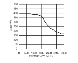
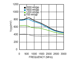
| 700 mVpp LVPECL CLOCK OUTPUTS (CLKoutX), CLKoutX_TYPE = 2 | ||||||
| VOH | Output high voltage | T = 25 °C, DC measurement Termination = 50 Ω to VCC - 1.4 V |
VCC - 1.03 | V | ||
| VOL | Output low voltage | VCC - 1.41 | V | |||
| VOD | Output voltage (see Figure 5) | 305 | 380 | 440 | |mV| | |
| VSS | 610 | 760 | 880 | mVpp | ||
| 1200 mVpp LVPECL CLOCK OUTPUTS (CLKoutX), CLKoutX_TYPE = 3 | ||||||
| VOH | Output high voltage | T = 25 °C, DC measurement Termination = 50 Ω to VCC - 1.7 V |
VCC - 1.07 | V | ||
| VOL | Output low voltage | VCC - 1.69 | V | |||
| VOD | Output voltage (see Figure 5) | 545 | 625 | 705 | |mV| | |
| VSS | 1090 | 1250 | 1410 | mVpp | ||
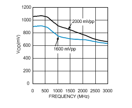
| 1600 mVpp LVPECL CLOCK OUTPUTS (CLKoutX), CLKoutX_TYPE = 4 | ||||||
| VOH | Output high voltage | T = 25 °C, DC Measurement Termination = 50 Ω to VCC - 2.0 V |
VCC - 1.10 | V | ||
| VOL | Output low voltage | VCC - 1.97 | V | |||
| VOD | Output voltage (see Figure 5) | 660 | 870 | 965 | |mV| | |
| VSS | 1320 | 1740 | 1930 | mVpp | ||
| 2000 mVpp LVPECL (2VPECL) CLOCK OUTPUTS (CLKoutX), CLKoutX_TYPE = 5 | ||||||
| VOH | Output high voltage | T = 25 °C, DC Measurement Termination = 50 Ω to VCC - 2.3 V |
VCC - 1.13 | V | ||
| VOL | Output low voltage | VCC - 2.20 | V | |||
| VOD | Output voltage Figure 5 | 800 | 1070 | 1200 | |mV| | |
| VSS | 1600 | 2140 | 2400 | mVpp | ||
| LVCMOS CLOCK OUTPUTS (CLKoutX) | ||||||
| fCLKout | Maximum frequency(18)(19) | 5 pF Load | 250 | MHz | ||
| VOH | Output high voltage | 1 mA Load | VCC - 0.1 | V | ||
| VOL | Output low voltage | 1 mA Load | 0.1 | V | ||
| IOH | Output high current (source) | VCC = 3.3 V, VO = 1.65 V | 28 | mA | ||
| IOL | Output low current (sink) | VCC = 3.3 V, VO = 1.65 V | 28 | mA | ||
| DUTYCLK | Output duty cycle(18) | VCC/2 to VCC/2, FCLK = 100 MHz T = 25 °C |
45% | 50% | 55% | |
| TR | Output rise time | 20% to 80%, RL = 50 Ω, CL = 5 pF |
400 | ps | ||
| TF | Output fall time | 80% to 20%, RL = 50 Ω, CL = 5 pF |
400 | ps | ||
| DIGITAL OUTPUTS (Status_CLKinX, Status_LD, Status_Holdover, SYNC) | ||||||
| VOH | High-Level output voltage | IOH = -500 µA | VCC - 0.4 | V | ||
| VOL | Low-Level output voltage | IOL = 500 µA | 0.4 | V | ||
| DIGITAL INPUTS (Status_CLKinX, SYNC) | ||||||
| VIH | High-Level input voltage | 1.6 | VCC | V | ||
| VIL | Low-Level input voltage | 0.4 | V | |||
| IIH | High-Level input current VIH = VCC |
Status_CLKinX_TYPE = 0 (High Impedance) |
-5 | 5 | µA | |
| Status_CLKinX_TYPE = 1 (Pull-up) |
-5 | 5 | ||||
| Status_CLKinX_TYPE = 2 (Pull-down) |
10 | 80 | ||||
| IIL | Low-Level input current VIL = 0 V |
Status_CLKinX_TYPE = 0 (High Impedance) |
-5 | 5 | µA | |
| Status_CLKinX_TYPE = 1 (Pull-up) |
-40 | -5 | ||||
| Status_CLKinX_TYPE = 2 (Pull-down) |
-5 | 5 | ||||
| DIGITAL INPUTS (CLKuWire, DATAuWire, LEuWire) | ||||||
| VIH | High-Level input voltage | 1.6 | VCC | V | ||
| VIL | Low-Level input voltage | 0.4 | V | |||
| IIH | High-Level input current | VIH = VCC | 5 | 25 | µA | |
| IIL | Low-Level input current | VIL = 0 | -5 | 5 | µA | |
(1) If emitter resistors are placed on the OSCout1/1* pins, there will be a DC current to ground which will cause powerdown Icc to increase.
(2) See Differential Voltage Measurement Terminology for definition of VID and VOD voltages.
(3) Load conditions for output clocks: LVDS: 100-Ω differential. See Current Consumption and Power Dissipation Calculations for Icc for specific part configuration and how to calculate Icc for a specific design.
(4) CLKin0, CLKin1 maximum is specified by characterization, production tested at 200 MHz.
(5) In order to meet the jitter performance listed in the subsequent sections of this data sheet, the minimum recommended slew rate for all input clocks is 0.5 V/ns. This is especially true for single-ended clocks. Phase noise performance will begin to degrade as the clock input slew rate is reduced. However, the device will function at slew rates down to the minimum listed. When compared to single-ended clocks, differential clocks (LVDS, LVPECL) will be less susceptible to degradation in phase noise performance at lower slew rates due to their common mode noise rejection. However, it is also recommended to use the highest possible slew rate for differential clocks to achieve optimal phase noise performance at the device outputs.
(6) This parameter is programmable
(7) FOSCin maximum frequency specified by characterization. Production tested at 200 MHz.
(8) The EN_PLL2_REF_2X bit (Register 13) enables/disables a frequency doubler mode for the PLL2 OSCin path.
(9) See Application Section discussion of Optional Crystal Oscillator Implementation (OSCin/OSCin*).
(10) A specification in modeling PLL in-band phase noise is the 1/f flicker noise, LPLL_flicker(f), which is dominant close to the carrier. Flicker noise has a 10 dB/decade slope. PN10kHz is normalized to a 10 kHz offset and a 1 GHz carrier frequency. PN10kHz = LPLL_flicker(10 kHz) - 20log(Fout / 1 GHz), where LPLL_flicker(f) is the single side band phase noise of only the flicker noise's contribution to total noise, L(f). To measure LPLL_flicker(f) it is important to be on the 10 dB/decade slope close to the carrier. A high compare frequency and a clean crystal are important to isolating this noise source from the total phase noise, L(f). LPLL_flicker(f) can be masked by the reference oscillator performance if a low power or noisy source is used. The total PLL in-band phase noise performance is the sum of LPLL_flicker(f) and LPLL_flat(f).
(11) A specification modeling PLL in-band phase noise. The normalized phase noise contribution of the PLL, LPLL_flat(f), is defined as: PN1HZ=LPLL_flat(f) - 20log(N) - 10log(fPDX). LPLL_flat(f) is the single side band phase noise measured at an offset frequency, f, in a 1 Hz bandwidth and fPDX is the phase detector frequency of the synthesizer. LPLL_flat(f) contributes to the total noise, L(f).
(12) Maximum Allowable Temperature Drift for Continuous Lock is how far the temperature can drift in either direction from the value it was at the time that the R30 register was last programmed, and still have the part stay in lock. The action of programming the R30 register, even to the same value, activates a frequency calibration routine. This implies the part will work over the entire frequency range, but if the temperature drifts more than the maximum allowable drift for continuous lock, then it will be necessary to reload the R30 register to ensure it stays in lock. Regardless of what temperature the part was initially programmed at, the temperature can never drift outside the frequency range of -40 °C to 85 °C without violating specifications.
(13) fVCO = 2949.12 MHz, PLL1 parameters: FPD1 = 1.024 MHz, ICP1 = 100 μA, loop bandwidth = 10 Hz. 122.88 MHz Crystek CVHD-950–122.880. PLL2 parameters: PLL2_R = 1, FPD2 = 122.88 MHz, ICP2 = 3200 μA, C1 = 47 pF, C2 = 3.9 nF, R2 = 620 Ω, PLL2_C3_LF = 0, PLL2_R3_LF = 0, PLL2_C4_LF = 0, PLL2_R4_LF = 0, CLKoutX_Y_DIV = 12, and CLKoutX_ADLY_SEL = 0.
(14) Equal loading and identical clock output configuration on each clock output is required for specification to be valid. Specification is not valid for CLKoutX or CLKoutY in analog delay mode.
(15) VCXO used is a 122.88 MHz Crystek CVHD-950-122.880.
(16) Crystal used is a 20.48 MHz Vectron VXB1-1150-20M480 and Skyworks varactor diode, SMV-1249-074LF.
(17) CLKout6 and OSCout0 also oscillate at start-up at the frequency of the VCXO attached to OSCin port.
(18) Specified by characterization.
(19) Refer to Typical Characteristics: Clock Output AC Characteristics for output operation performance at higher frequencies than the minimum maximum output frequency.
6.6 Timing Requirements
See Serial MICROWIRE Timing Diagram and Advanced MICROWIRE Timing Diagrams for additional information| MIN | NOM | MAX | UNIT | |||
|---|---|---|---|---|---|---|
| TECS | LE to Clock Set Up Time | See Figure 6 | 25 | ns | ||
| TDCS | Data to Clock Set Up Time | See Figure 6 | 25 | ns | ||
| TCDH | Clock to Data Hold Time | See Figure 6 | 8 | ns | ||
| TCWH | Clock Pulse Width High | See Figure 6 | 25 | ns | ||
| TCWL | Clock Pulse Width Low | See Figure 6 | 25 | ns | ||
| TCES | Clock to LE Set Up Time | See Figure 6 | 25 | ns | ||
| TEWH | LE Pulse Width | See Figure 6 | 25 | ns | ||
| TCR | Falling Clock to Readback Time | See Figure 9 | 25 | ns |
6.7 Typical Characteristics: Clock Output AC Characteristics