SNAS521H July 2011 – January 2016 LMP90077 , LMP90078 , LMP90079 , LMP90080
PRODUCTION DATA.
- 1 Features
- 2 Applications
- 3 Description
- 4 Revision History
- 5 Description (continued)
- 6 Device Comparison Table
- 7 Pin Configuration and Functions
-
8 Specifications
- 8.1 Absolute Maximum Ratings
- 8.2 ESD Ratings
- 8.3 Recommended Operating Conditions
- 8.4 Thermal Information
- 8.5 Electrical Characteristics
- 8.6 Timing Requirements
- 8.7 Timing Requirements - CSB Timing
- 8.8 Timing Requirements - SCLK and SDI Timing
- 8.9 Timing Requirements - SDO Timing With DOD1
- 8.10 Timing Requirements - SDO Timing with DOD2
- 8.11 Timing Requirements - SDO and DRDYB Timing
- 8.12 Typical Characteristics
-
9 Detailed Description
- 9.1 Overview
- 9.2 Functional Block Diagram
- 9.3
Feature Description
- 9.3.1 Calibration
- 9.3.2 True Continuous Background Calibration
- 9.3.3 Continuous Background Sensor Diagnostics
- 9.3.4 Flexible Input MUX Channels
- 9.3.5 Programmable Gain Amplifiers (FGA & PGA)
- 9.3.6 Excitation Current Sources (IB1 & IB2) - LMP90080/LMP90078
- 9.3.7 Signal Path
- 9.4 Device Functional Modes
- 9.5
Programming
- 9.5.1 Serial Digital Interface
- 9.5.2 RESET and RESTART
- 9.5.3 Register Read/Write Examples
- 9.5.4 Streaming Examples
- 9.6 Register Maps
- 10Application and Implementation
- 11Power Supply Recommendations
- 12Layout
- 13Device and Documentation Support
- 14Mechanical, Packaging, and Orderable Information
パッケージ・オプション
メカニカル・データ(パッケージ|ピン)
- PWP|28
サーマルパッド・メカニカル・データ
- PWP|28
発注情報
10 Application and Implementation
NOTE
Information in the following applications sections is not part of the TI component specification, and TI does not warrant its accuracy or completeness. TI’s customers are responsible for determining suitability of components for their purposes. Customers should validate and test their design implementation to confirm system functionality.
10.1 Application Information
10.1.1 Connecting the Supplies
10.1.1.1 VA and VIO
Any ADC architecture is sensitive to spikes on the analog voltage, VA, digital input/output voltage, VIO, and ground pins. These spikes may originate from switching power supplies, digital logic, high power devices, and other sources. To diminish these spikes, the LMP900xx’s VA and VIO pins should be clean and well bypassed. A 0.1 µF ceramic bypass capacitor and a 1 µF tantalum capacitor should be used to bypass the LMP900xx supplies, with the 0.1 µF capacitor placed as close to the LMP900xx as possible.
Since the LMP900xx has both external VA and VIO pins, the user has two options on how to connect these pins. The first option is to tie VA and VIO together and power them with the same power supply. This is the most cost effective way of powering the LMP900xx but is also the least ideal because noise from VIO can couple into VA and negatively affect performance. The second option involves powering VA and VIO with separate power supplies. These supply voltages can have the same amplitude or they can be different.
10.1.1.2 VREF
Operation with VREF below VA is also possible with slightly diminished performance. As VREF is reduced, the range of acceptable analog input voltages is also reduced. Reducing the value of VREF also reduces the size of the LSB. When the LSB size goes below the noise floor of the LMP900xx, the noise will span an increasing number of codes and performance will degrade. For optimal performance, VREF should be the same as VA and sourced with a clean source that is bypassed with a ceramic capacitor value of 0.1 µF and a tantalum capacitor of 10 µF.
LMP900xx also allows ratiometric connection for noise immunity reasons. A ratiometric connection is when the ADC’s VREFP and VREFN are used to excite the input device’s (i.e. a bridge sensor) voltage references. This type of connection severely attenuates any VREF ripple seen the ADC output, and is thus strongly recommended.
10.1.2 Quick Start
This section shows step-by-step instructions to configure the LMP900xx to perform a simple DC reading from CH0.
- Apply VA = VIO = VREFP1 = 5V, and ground VREFN1
- Apply VINP = ¾VREF and VINN = ¼VREF for CH0. Thus, set CH0 = VIN = VINP - VINN = ½VREF (CH0_INPUTCN register)
- Set gain = 1 (CH0_CONFIG: GAIN_SEL = 0x0)
- Exclude the buffer from the signal path (CH0_CONFIG: BUF_EN = 0)
- Set the background to BgcalMode2 (BGCALCN = 0x2)
- Select VREF1 (CH0_INPUTCN: VREF_SEL = 0)
- To use the internal CLK, set CLK_EXT_DET = 1 and CLK_SEL = 0.
- Follow the register read/write protocol (Figure 55) to capture ADC_DOUT from CH0.
10.1.3 ADC_DOUT Calculation
The output code of the LMP900xx can be calculated as:

ADC_DOUT is in 16−bit two's complement binary format. The largest positive value is 0x7FFF (or 32767 in decimal), while the largest negative value is 0x8000 (or 32768 in decimal). In case of an over range the value is automatically clamped to one of these two values.
Figure 71 shows the theoretical output code, ADC_DOUT, vs. analog input voltage, VIN, using the equation above.
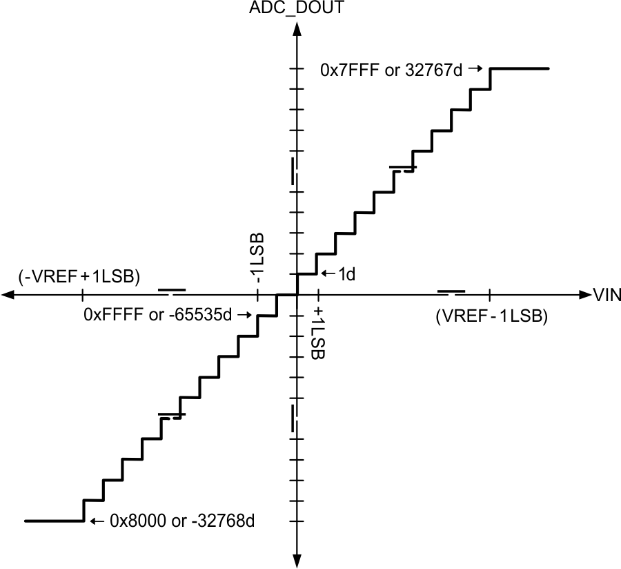 Figure 71. ADC_DOUT vs. VIN of a 16-Bit Resolution (VREF = 5.5 V, Gain = 1).
10.2 Typical Applications
10.2.1 Typical Sensor Application
 Figure 72. Typical Sensor Application
10.2.1.1 Design Requirements
- VA = 3 V
- VIO = 3 V
- 3-Wire RTD using 2 current sources
10.2.1.2 Detailed Design Procedure
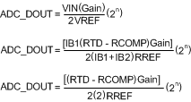
Figure 72 shows the first topology for a 3-wire resistive temperature detector (RTD) application. Topology #1 uses two excitation current sources, IB1 and IB2, to create a differential voltage across VIN0 and VIN1. As a result of using both IB1 and IB2, only one channel (VIN0-VIN1) needs to be measured. As shown in Equation 14, the equation for this channel is IB1 x (RTD – RCOMP) assuming that RLINE1 = RLINE2.

The PT-100 changes linearly from 100 Ω at 0°C to 146.07 Ω at 120°C. If desired, choose a suitable compensating resistor (RCOMP) so that VIN can be virtually 0 V at any desirable temperature. For example, if RCOMP = 100 Ω, then at 0°C, VIN = 0 V and thus a higher gain can be used.
The advantage of this circuit is its ratiometric configuration, where VREF = (IB1 + IB2) x (RREF). Equation 15 shows that a ratiometric configuration eliminates IB1 and IB2 from the output equation, thus increasing the overall performance.
10.2.1.3 Application Curve
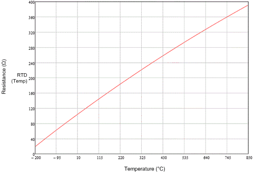 Figure 73. PT-100 RTD Resistance from –200°C to 850°C
10.2.2 3–Wire RTD
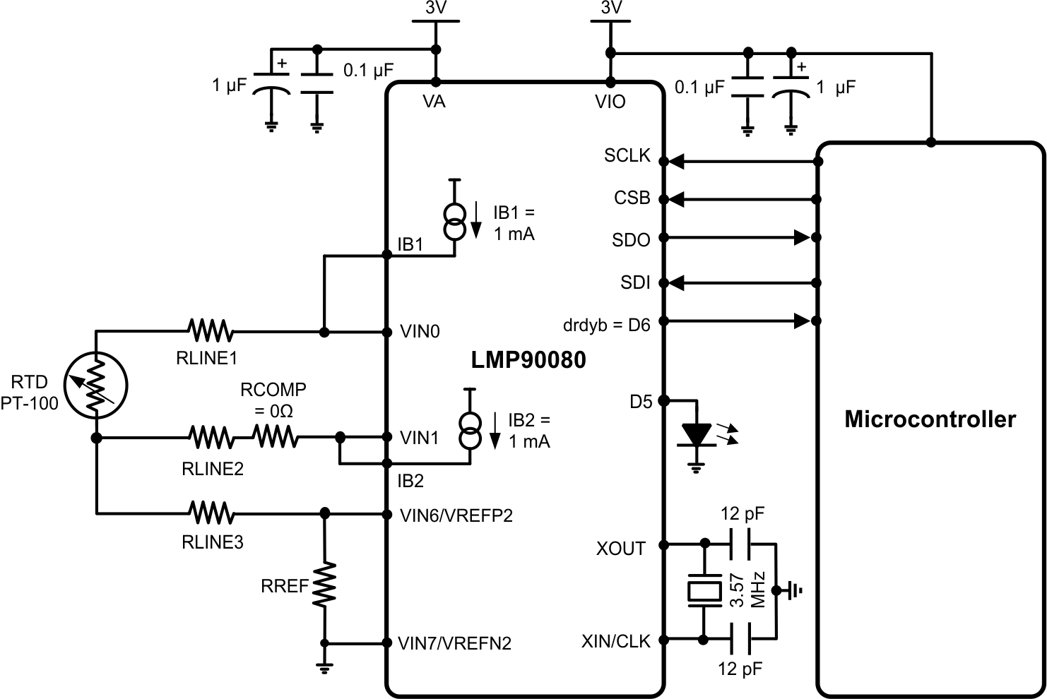 Figure 74. Topology #1: 3-Wire RTD using 2 Current Sources
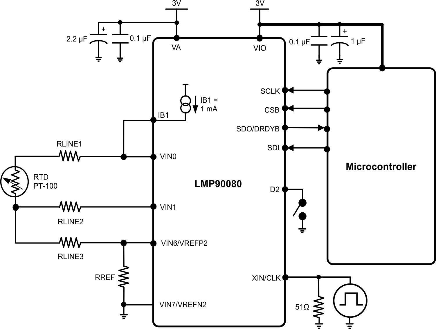 Figure 75. Topology #2: 3-Wire RTD using 1 Current Source
10.2.2.1 Design Requirements
- VA = 3V
- VIO = 3V
- 3-Wire RTD using 1 current source
10.2.2.2 Detailed Design Procedure
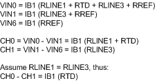
Figure 75 shows the second topology for a 3-Wire RTD application. Topology #2 shows the same connection as topology #1, but without IB2. Although this topology eliminates a current source, it requires two channel measurements as shown in Equation 16.
10.2.2.3 Application Curve
 Figure 76. PT-100 RTD Resistance from –200°C to 850°C
10.2.3 Thermocouple and IC Analog Temperature
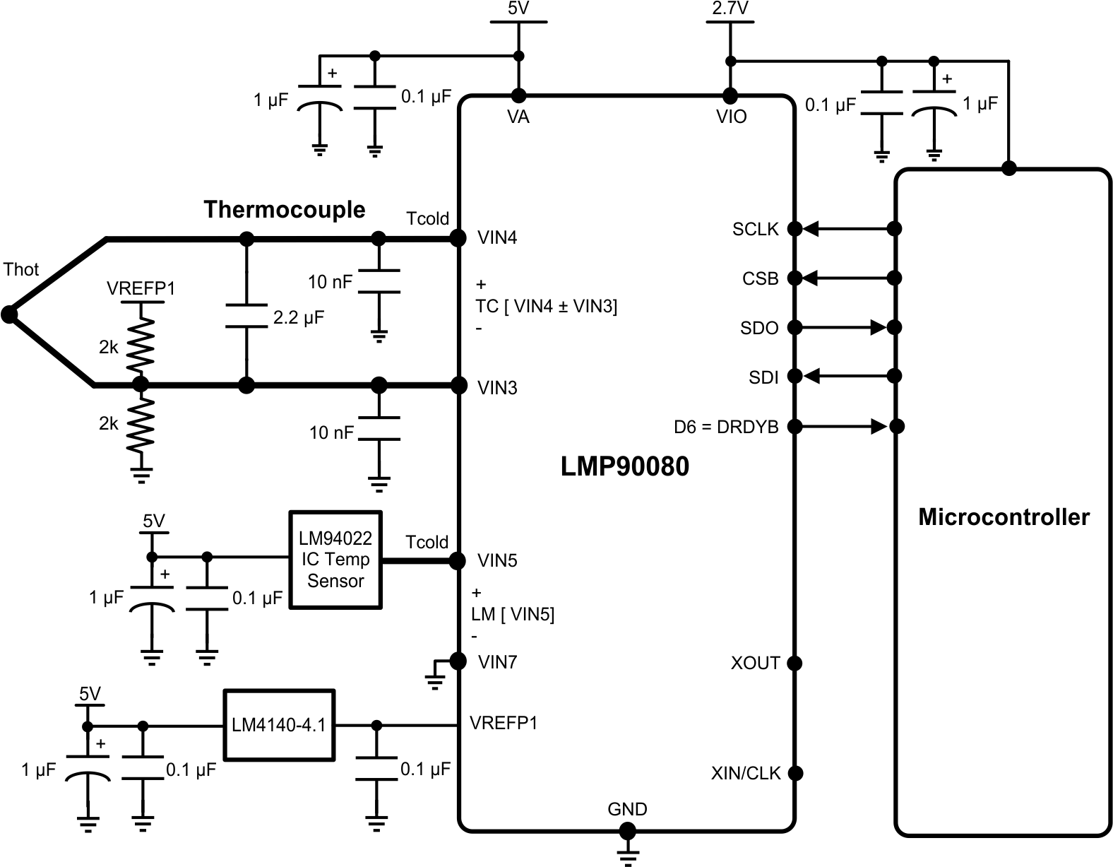 Figure 77. Thermocouple with CJC
10.2.3.1 Design Requirements
- VA = 5V
- VIO = 2.7V
- Thermocouple with Cold Junction Compensation
10.2.3.2 Detailed Design Procedure
The LMP900xx is also ideal for thermocouple temperature applications. Thermocouples have several advantages that make them popular in many industrial and medical applications. Compare to RTDs, thermistors, and IC sensors, thermocouples are the most rugged, least expensive, and can operate over the largest temperature range.
A thermocouple is a sensor whose junction generates a differential voltage, VIN, that is relative to the temperature difference (Thot – Tcold). Thot is also known as the measuring junction or “hot” junction, which is placed at the measured environment. Tcold is also known as the reference or “cold” junction, which is placed at the measuring system environment.
Because a thermocouple can only measure a temperature difference, it does not have the ability to measure absolute temperature. To determine the absolute temperature of the measured environment (Thot), a technique known as cold junction compensation (CJC) must be used.
In a CJC technique, the “cold” junction temperature, Tcold, is sensed by using an IC temperature sensor, such as the LM94022. The temperature sensor should be placed within close proximity of the reference junction and should have an isothermal connection to the board to minimize any potential temperature gradients.
Once Tcold is obtained, use a standard thermocouple look-up-table to find its equivalent voltage. Next, measure the differential thermocouple voltage and add the equivalent cold junction voltage. Lastly, convert the resulting voltage to temperature using a standard thermocouple look-up-table.
For example, assume Tcold = 20°C. The equivalent voltage from a type K thermocouple look-up-table is 0.798 mV. Next, add the measured differential thermocouple voltage to the Tcold equivalent voltage. For example, if the thermocouple voltage is 4.096 mV, the total would be 0.798 mV + 4.096 mV = 4.894 mV. Referring to the type K thermocouple table gives a temperature of 119.37°C for 4.894 mV.
10.2.3.3 Application Curve
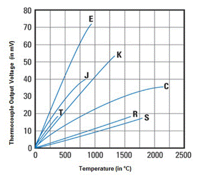 Figure 78. Thermocouple Output as Function of Temperature