SNAS236G October 2005 – January 2016 LMX2485 , LMX2485E
PRODUCTION DATA.
- 1 Features
- 2 Applications
- 3 Description
- 4 Revision History
- 5 Pin Configuration and Functions
- 6 Specifications
- 7 Parameter Measurement Information
-
8 Detailed Description
- 8.1 Overview
- 8.2 Functional Block Diagram
- 8.3
Feature Description
- 8.3.1 TCXO, Oscillator Buffer, and R Counter
- 8.3.2 Phase Detector
- 8.3.3 Charge Pump
- 8.3.4 Loop Filter
- 8.3.5 N Counters and High Frequency Input Pins
- 8.3.6 Digital Lock Detect Operation
- 8.3.7 Cycle Slip Reduction and Fastlock
- 8.3.8 Fractional Spur and Phase Noise Controls
- 8.4 Device Functional Modes
- 8.5 Programming
- 8.6
Register Maps
- 8.6.1 R0 Register
- 8.6.2 R1 Register
- 8.6.3 R2 Register
- 8.6.4 R3 Register
- 8.6.5
R4 Register
- 8.6.5.1 MUX[3:0] Frequency Out and Lock Detect MUX
- 8.6.5.2 IF_P—IF Prescaler
- 8.6.5.3 RF_CPP—RF PLL Charge Pump Polarity
- 8.6.5.4 IF_CPP—IF PLL Charge Pump Polarity
- 8.6.5.5 OSC_OUT Oscillator Output Buffer Enable
- 8.6.5.6 OSC2X—Oscillator Doubler Enable
- 8.6.5.7 FM[1:0]—Fractional Mode
- 8.6.5.8 DITH[1:0]—Dithering Control
- 8.6.5.9 ATPU—PLL Automatic Power Up
- 8.6.6 R5 Register
- 8.6.7 R6 Register
- 8.6.8 R7 Register
- 9 Application and Implementation
- 10Power Supply Recommendations
- 11Layout
- 12Device and Documentation Support
- 13Mechanical, Packaging, and Orderable Information
7 Parameter Measurement Information
7.1 Bench Test Set-Ups
7.1.1 Charge Pump Current Measurement
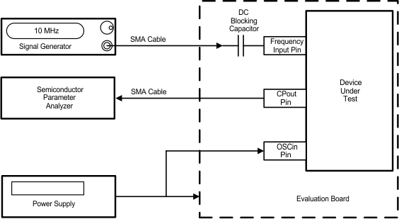 Figure 19. Charge Pump Current Measurement
Figure 19 shows the test procedure for testing the RF and IF charge pumps. These tests include absolute current level, mismatch, and leakage measurement. To measure the charge pump currents, a signal is applied to the high frequency input pins. The reason for this is to guarantee that the phase detector gets enough transitions to be able to change states. If no signal is applied, it is possible that the charge pump current reading will be low due to the fact that the duty cycle is not 100%. The OSCin Pin is tied to the supply. The charge pump currents can be measured by simply programming the phase detector to the necessary polarity. For instance, to measure the RF charge pump, a 10 MHz signal is applied to the FinRF pin. The source current can be measured by setting the RF PLL phase detector to a positive polarity, and the sink current can be measured by setting the phase detector to a negative polarity. The IF PLL currents can be measured in a similar way. The magnitude of the RF PLL charge pump current is controlled by the RF_CPG bit. Once the charge pump currents are known, the mismatch can be calculated as well. To measure leakage, the charge pump is set to a TRI-STATE mode by enabling the RF_CPT and IF_CPT bits. Table 4 shows a summary of the various charge pump tests.
Table 4. Programmable Settings for Charge Pump Current Tests
| CURRENT TEST | RF_CPG | RF_CPP | RF_CPT | IF_CPP | IF_CPT |
|---|---|---|---|---|---|
| RF Source | 0 to 15 | 0 | 0 | X | X |
| RF Sink | 0 to 15 | 1 | 0 | X | X |
| RF TRI-STATE | X | X | 1 | X | X |
| IF Source | X | X | X | 0 | 0 |
| IF Sink | X | X | X | 1 | 0 |
| IF TRI-STATE | X | X | X | X | 1 |
7.1.2 Charge Pump Current Specification Definitions
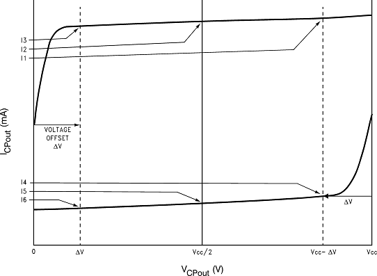 Figure 20. Charge Pump Current Specification Definitions
I1 = Charge Pump Sink Current at VCPout = Vcc - ΔV
I2 = Charge Pump Sink Current at VCPout = Vcc/2
I3 = Charge Pump Sink Current at VCPout = ΔV
I4 = Charge Pump Source Current at VCPout = Vcc - ΔV
I5 = Charge Pump Source Current at VCPout = Vcc/2
I6 = Charge Pump Source Current at VCPout = ΔV
ΔV = Voltage offset from the positive and negative supply rails. Defined to be 0.5 V for this part.
vCPout refers to either VCPoutRF or VCPoutIF
ICPout refers to either ICPoutRF or ICPoutIF
7.1.2.1 Charge Pump Output Current Magnitude Variation vs Charge Pump Output Voltage
Use Equation 1 to calculate the charge pump output current variation versus the charge pump output voltage.
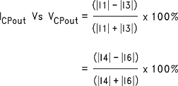
7.1.2.2 Charge Pump Sink Current vs Charge Pump Output Source Current Mismatch
Use Equation 2 to calculate the charge pump sink current versus the source current mismatch.

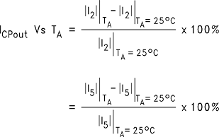
7.1.2.3 Charge Pump Output Current Magnitude Variation vs Temperature
Use Equation 3 to calculate the charge pump output current magnitude variation versus the temperature.
7.1.3 Sensitivity Measurement Procedure
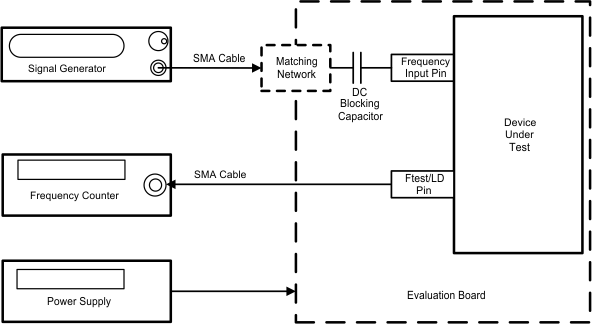 Figure 21. Setup for Sensitivity Measurement
Table 5. Sensitivity Set-Up Diagram
| FREQUENCY INPUT PIN | DC-BLOCKING CAPACITOR | CORRESPONDING COUNTER | DEFAULT COUNTER VALUE | MUX VALUE |
|---|---|---|---|---|
| OSCin | 1000 pF | RF_R / 2 | 50 | 14 |
| FinRF | 100 pF// 1000 pF | RF_N / 2 | 502 + 2097150 / 4194301 | 15 |
| FinIF | 100 pF | IF_N / 2 | 534 | 13 |
| OSCin | 1000 pF | IF_R / 2 | 50 | 12 |
Sensitivity is defined as the power level limits beyond which the output of the counter being tested is off by 1 Hz or more of its expected value. It is typically measured over frequency, voltage, and temperature. To test sensitivity, the MUX[3:0] word is programmed to the appropriate value. The counter value is then programmed to a fixed value and a frequency counter is set to monitor the frequency of this pin. The expected frequency at the Ftest/LD pin should be the signal generator frequency divided by twice the corresponding counter value. The factor of two comes in because the LMX2485 has a flip-flop which divides this frequency by two to make the duty cycle 50% to make it easier to read with the frequency counter. The frequency counter input impedance should be set to high impedance. To perform the measurement, the temperature, frequency, and voltage is set to a fixed value and the power level of the signal is varied. If the power level at the part is assumed to be 4 dB less than the signal generator power level. This accounts for 1 dB for cable losses and 3 dB for the pad. The power level range where the frequency is correct at the Ftest/LD pin to within 1 Hz accuracy is recorded for the sensitivity limits. The temperature, frequency, and voltage can be varied to produce a family of sensitivity curves. Because this is an open-loop test, the charge pump is set to TRI-STATE and the unused side of the PLL (RF or IF) is powered down when not being tested. For this part, there are actually four frequency input pins, although there is only one frequency test pin (Ftest/LD). The conditions specific to each pin are shown in Table 5.
NOTE
For the RF N counter, a fourth order fractional modulator is used in 22-bit mode with a fraction of 2097150 / 4194301 is used. The reason for this long fraction is to test the RF N counter and supporting fractional circuitry as completely as possible.
7.1.4 Input Impedance Measurement
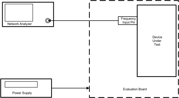 Figure 22. Input Impedance Measurement
Figure 22 shows the test set-up used for measuring the input impedance for the LMX2485. The DC-blocking capacitor used between the input SMA connector and the pin being measured must be changed to a 0-Ω resistor. This procedure applies to the FinRF, FinIF, and OSCin pins. The basic test procedure is to calibrate the network analyzer, ensure that the part is powered up, and then measure the input impedance. The network analyzer can be calibrated by using either calibration standards or by soldering resistors directly to the evaluation board. An open can be implemented by putting no resistor, a short can be implemented by soldering a 0-Ω resistor as close as possible to the pin being measured, and a short can be implemented by soldering two 100-Ω resistors in parallel as close as possible to the pin being measured. Calibration is done with the PLL removed from the PCB. This requires the use of a clamp down fixture that may not always be generally available. If no clamp down fixture is available, then this procedure can be done by calibrating up to the point where the DC-blocking capacitor usually is, and then implementing port extensions with the network analyzer. The 0-Ω resistor is added back for the actual measurement. Once the set-up is calibrated, it is necessary to ensure that the PLL is powered up. This can be done by toggling the power down bits (RF_PD and IF_PD) and observing that the current consumption indeed increases when the bit is disabled. Sometimes it may be necessary to apply a signal to the OSCin pin to program the part. If this is necessary, disconnect the signal once it is established that the part is powered up. It is useful to know the input impedance of the PLL for the purposes of debugging RF problems and designing matching networks. Another use of knowing this parameter is make the trace width on the PCB such that the input impedance of this trace matches the real part of the input impedance of the PLL frequency of operation. In general, it is good practice to keep trace lengths short and make designs that are relatively resistant to variations in the input impedance of the PLL.