SNAS236G October 2005 – January 2016 LMX2485 , LMX2485E
PRODUCTION DATA.
- 1 Features
- 2 Applications
- 3 Description
- 4 Revision History
- 5 Pin Configuration and Functions
- 6 Specifications
- 7 Parameter Measurement Information
-
8 Detailed Description
- 8.1 Overview
- 8.2 Functional Block Diagram
- 8.3
Feature Description
- 8.3.1 TCXO, Oscillator Buffer, and R Counter
- 8.3.2 Phase Detector
- 8.3.3 Charge Pump
- 8.3.4 Loop Filter
- 8.3.5 N Counters and High Frequency Input Pins
- 8.3.6 Digital Lock Detect Operation
- 8.3.7 Cycle Slip Reduction and Fastlock
- 8.3.8 Fractional Spur and Phase Noise Controls
- 8.4 Device Functional Modes
- 8.5 Programming
- 8.6
Register Maps
- 8.6.1 R0 Register
- 8.6.2 R1 Register
- 8.6.3 R2 Register
- 8.6.4 R3 Register
- 8.6.5
R4 Register
- 8.6.5.1 MUX[3:0] Frequency Out and Lock Detect MUX
- 8.6.5.2 IF_P—IF Prescaler
- 8.6.5.3 RF_CPP—RF PLL Charge Pump Polarity
- 8.6.5.4 IF_CPP—IF PLL Charge Pump Polarity
- 8.6.5.5 OSC_OUT Oscillator Output Buffer Enable
- 8.6.5.6 OSC2X—Oscillator Doubler Enable
- 8.6.5.7 FM[1:0]—Fractional Mode
- 8.6.5.8 DITH[1:0]—Dithering Control
- 8.6.5.9 ATPU—PLL Automatic Power Up
- 8.6.6 R5 Register
- 8.6.7 R6 Register
- 8.6.8 R7 Register
- 9 Application and Implementation
- 10Power Supply Recommendations
- 11Layout
- 12Device and Documentation Support
- 13Mechanical, Packaging, and Orderable Information
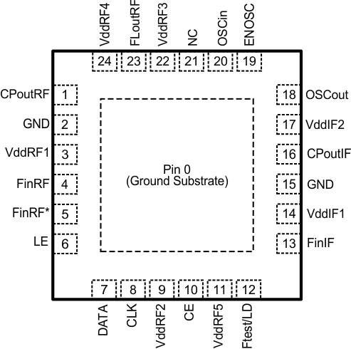
5 Pin Configuration and Functions
RTW Package
24-Pin WQFN
Top View

Pin Functions
| PIN | I/O | DESCRIPTION | |
|---|---|---|---|
| NO. | NAME | ||
| 0 | GND | — | Ground substrate; this is on the bottom of the package and must be grounded. |
| 1 | CPoutRF | O | RF PLL charge pump output |
| 2 | GND | — | RF PLL analog ground |
| 3 | VddRF1 | — | RF PLL analog power supply |
| 4 | FinRF | I | RF PLL high-frequency input pin |
| 5 | FinRF* | I | RF PLL complementary high-frequency input pin; shunt to ground with a 100-pF capacitor. |
| 6 | LE | I | MICROWIRE load enable; high-impedance CMOS input. Data stored in the shift registers is loaded into the internal latches when LE goes HIGH. |
| 7 | DATA | I | MICROWIRE data; high-impedance binary serial data input. |
| 8 | CLK | I | MICROWIRE clock; high-impedance CMOS Clock input. Data for the various counters is clocked into the 24-bit shift register on the rising edge. |
| 9 | VddRF2 | — | Power supply for RF PLL digital circuitry |
| 10 | CE | I | Chip Enable control pin; must be pulled high for normal operation. |
| 11 | VddRF5 | I | Power supply for RF PLL circuitry |
| 12 | Ftest/LD | O | Test frequency output / lock detect |
| 13 | FinIF | I | IF PLL high-frequency input pin |
| 14 | VddIF1 | — | IF PLL analog power supply |
| 15 | GND | — | IF PLL digital ground |
| 16 | CPoutIF | O | IF PLL charge pump output |
| 17 | VddIF2 | — | IF PLL power supply |
| 18 | OSCout | O | Buffered output of the OSCin signal |
| 19 | ENOSC | I | Oscillator enable; when this is set to high, the OSCout pin is enabled regardless of the state of other pins or register bits. |
| 20 | OSCin | I | Input for TCXO signal |
| 21 | NC | I | This pin must be left open. |
| 22 | VddRF3 | — | Power supply for RF PLL digital circuitry |
| 23 | FLoutRF | O | RF PLL fastlock output; also functions as programmable TRI-STATE CMOS output. |
| 24 | VddRF4 | — | RF PLL analog power supply |