JAJSCK2A October 2016 – January 2017 LMX2491
PRODUCTION DATA.
- 1 特長
- 2 アプリケーション
- 3 概要
- 4 改訂履歴
- 5 Pin Configuration and Functions
- 6 Specifications
-
7 Detailed Description
- 7.1 Overview
- 7.2 Functional Block Diagram
- 7.3
Feature Description
- 7.3.1 OSCin Input
- 7.3.2 OSCin Doubler
- 7.3.3 R Divider
- 7.3.4 PLL N Divider
- 7.3.5 Fractional Circuitry
- 7.3.6 PLL Phase Detector and Charge Pump
- 7.3.7 External Loop Filter
- 7.3.8 Fastlock and Cycle Slip Reduction
- 7.3.9 Lock Detect and Charge Pump Voltage Monitor
- 7.3.10 FSK/PSK Modulation
- 7.3.11 Ramping Functions
- 7.3.12 Power-on-reset (POR)
- 7.3.13 Register Readback
- 7.4 Device Functional Modes
- 7.5 Programming
- 7.6 Register Maps
-
8 Applications and Implementation
- 8.1 Application Information
- 8.2
Typical Application
- 8.2.1 Design Requirements
- 8.2.2 Detailed Design Procedure
- 8.2.3 TICS Pro Basic Setup
- 8.2.4 Frequency Shift Keying Example
- 8.2.5 Single Sawtooth Ramp Example
- 8.2.6 Continuous Sawtooth Ramp Example
- 8.2.7 Continuous Sawtooth Ramp with FSK Example
- 8.2.8 Continuous Triangular Ramp Example
- 8.2.9 Continuous Trapezoid Ramp Example
- 8.2.10 Arbitrary Waveform Ramp Example
- 9 Power Supply Recommendations
- 10Layout
- 11デバイスおよびドキュメントのサポート
- 12メカニカル、パッケージ、および注文情報
パッケージ・オプション
メカニカル・データ(パッケージ|ピン)
- RTW|24
サーマルパッド・メカニカル・データ
- RTW|24
発注情報
8 Applications and Implementation
NOTE
Information in the following applications sections is not part of the TI component specification, and TI does not warrant its accuracy or completeness. TI’s customers are responsible for determining suitability of components for their purposes. Customers should validate and test their design implementation to confirm system functionality.
8.1 Application Information
The LMX2491 can be used in a broad class of applications such as generating a single frequency for a high frequency clock, generating a tunable range of frequencies, or generating swept waveforms that can be used in applications such as radar.
8.2 Typical Application
Figure 14 is an example that could be used in a typical application.
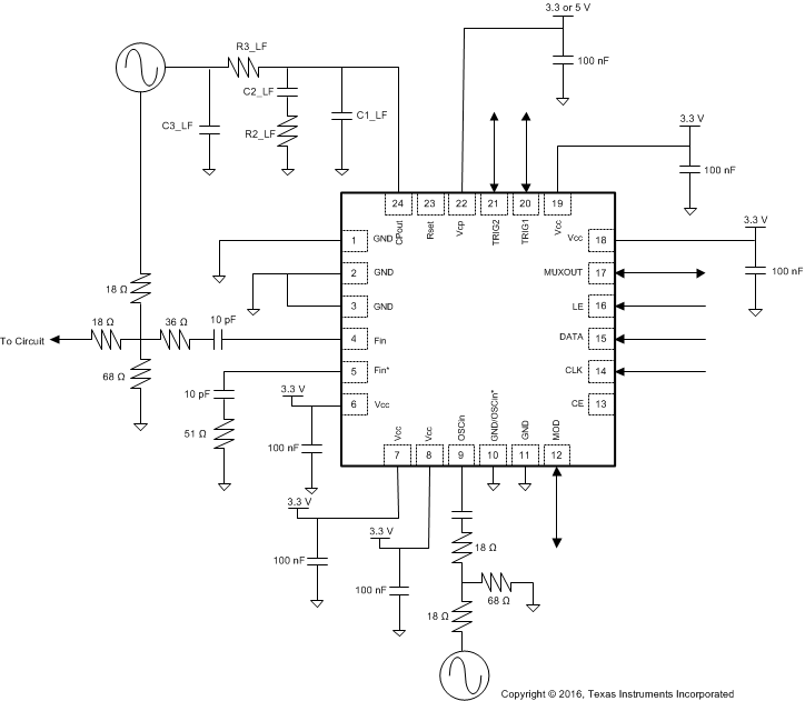 Figure 14. Typical Schematic
8.2.1 Design Requirements
For these examples, it will be assumed that there is a 100 MHz input signal and the output frequency is between 1500 and 1520 MHz with various modulated waveforms.
Table 18. Design Requirements
| PARAMETER | SYMBOL | VALUE | COMMENTS |
|---|---|---|---|
| Input frequency | fOSCin | 100 MHz | |
| Phase detector frequency | fPD | 50 MHz | There are many possibilities, but this choice gives good performance. |
| VCO frequency | fVCO | 1500 - 1520 MHz | In the different examples, the VCO frequency is actually changing. However, the same loop filter design can be used for all examples. Unmodulated VCO frequency or steady state VCO frequency without ramp is 1500 MHz. |
| VCO gain | KVCO | 65 MHz/V | This parameter has nothing to do with the LMX2491, but is rather set by the external VCO choice. |
8.2.2 Detailed Design Procedure
The first step is to calculate the reference divider (PLL_R) and feedback divider (PLL_N) values as shown in the table that follows.
Table 19. Detailed Design Procedure
| PARAMETER | SYMBOL AND CALCULATIONS | VALUE | COMMENTS |
|---|---|---|---|
| Average VCO frequency | fVCOavg = (fVCOmax + fVCOmin) / 2 | 1510 MHz | To design a loop filter, one designs for a fixed VCO value, although it is understood that the VCO will tune around. This typical value is usually chosen as the average VCO frequency |
| VCO gain | KVCO | 65 MHz/V | This parameter has nothing to do with LMX2491, but is rather set by the external VCO choice. In this case, it was the CVCO55BE-1400-1624 VCO. |
| VCO input capacitance | CVCO | 120 pF | This parameter has nothing to do with LMX2491, but is rather set by the external VCO choice. |
| PLL loop bandwidth | LBW | 380 kHz | This bandwidth is very wide to allow the VCO frequency to be modulated. |
| Charge pump gain | CPG | 3.1 mA | Using the larger gain allows a wider loop bandwidth and gives good phase performance. |
| R-divider | PLL_R = fOSCin / fPD | 2 | |
| N-divider | PLL_N = fVCO / fPD | 96 | |
| Loop filter components | C1_LF | 68 pF | These were calculated by TI PLLatinum Simulator Tool. |
| C2_LF | 3.9 nF | ||
| C3_LF | 150 pF | ||
| R2_LF | 390 Ω | ||
| R3_LF | 150 Ω |
Once a loop filter bandwidth is chosen, the external loop filter component values can be calculated with a tool such as PLLatinum Simulator Tool. It is also highly recommended to look at the EVM User's Guide. TICS Pro software is an excellent starting point and example to see how to program this device.
8.2.3 TICS Pro Basic Setup
In the following application examples, TICS Pro is used to program the device to implement different ramp profiles. The following procedure shows how to setup TICS Pro to put the device to lock to 1500 MHz without modulation or ramp.
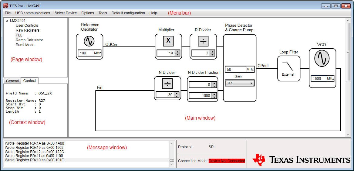 Figure 15. TICS Pro
- In the Menu bar, click Select Device and then select LMX2491.
- In the Menu bar, click Default Configuration and then select Default Mode.
- In the Page window, click PLL.
- In the Main window, change R Divider value to 2 and VCO value to 1500.
- In the Menu bar, click USB Communications and then click Write All Registers. The device is now locked to 1500 MHz.
Other TICS Pro fundamentals:
- When a particular content in the Main window is moused-over, the Context window will show a brief description of that content.
- An alternative method to write all registers is press the Ctrl key and L key from the keyboard.
- Whenever a value is updated in the Main window, the Message window will show which register is being updated
8.2.4 Frequency Shift Keying Example
FSK operation requires an external input trigger signal at either MOD, TRIG1 or TRIG2 pin. In this example, MOD pin is selected as the Trigger A source. A 20 kHz square-wave clock will be applied to MOD pin to toggle the RF output to switch between 1500 MHz and 1502 MHz. That is, FSK frequency deviation is 2 MHz. The following register bits are required to set in order to initiate FSK operation.
Table 20. FSK Register Settings
| PARAMETER | REGISTER BIT | SETTING | COMMENTS |
|---|---|---|---|
| Frequency deviation | FSK_DEV | 671089 = 2 MHz | Frequency deviation = (fPD x FSK_DEV) / 224 |
| MOD pin characteristic | MOD_PIN | 7 = Input | Set MOD pin as an input pin |
| FSK trigger source | FSK_DEV_TRIG | 1 = Trigger A | Use Trigger A to trigger FSK |
| Trigger source definition | RAMP_TRIGA | 3 = MOD Rising Edge | When there is a L-to-H transition at MOD pin, the set amount of frequency deviation will be added to the unmodulated carrier |
| Enable ramp | RAMP_EN | 1 = Enabled | Activate FSK operation |
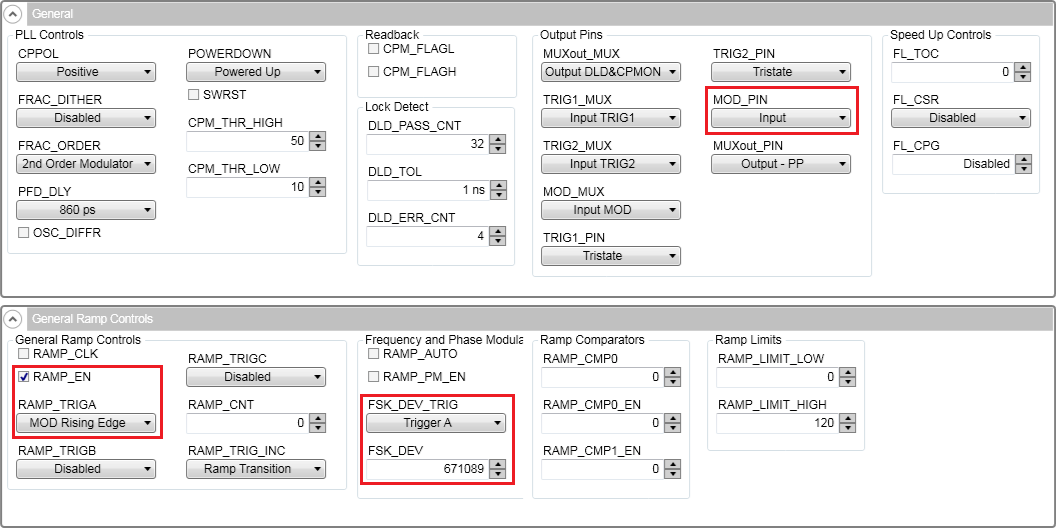 Figure 16. TICS Pro FSK Configuration
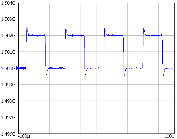 Figure 17. Frequency Shift Keying Example
8.2.5 Single Sawtooth Ramp Example
In this example, Trigger B is used to trigger the ramp generator of LMX2491 to general a single frequency ramp between 1500 MHz and 1520 MHz. Ramp duration is 50 µs. The ramp will finish and return back to 1500 MHz immediately when the output frequency reaches 1520 MHz. Trigger 1 pin is assigned as Trigger B source.
Two ramp segments are setup to create this one-time single ramp. RAMP0 is used to establish a trigger for the second ramp segment - RAMP1. When a trigger signal is received, RAMP1 will execute and bring the output frequency to 1520 MHz in 50 µs.
Table 21. Single Sawtooth Ramp Register Settings
| PARAMETER | REGISTER BIT | SETTING | COMMENTS |
|---|---|---|---|
| Set maximum ramp frequency threshold | RAMP_LIMIT_HIGH | 16777216 = 1550 MHz | This threshold frequency can be anything above 1520 MHz. The fractional numerator is equal to 0 at 1550 MHz. The N-Divider difference between 1500 MHz and 1550 MHz is 1. From Equation 1, this threshold is equal to 0 + (1 x 224) = 16777216. |
| Set minimum ramp frequency threshold | RAMP_LIMIT_LOW | 8573157376 = 1450 MHz | This threshold frequency can be anything below 1500 MHz. This threshold is equal to –16777216. This is a 33-bit long register, 2's complement is therefore equal to 8573157376. |
| Number of ramp in each ramp segment | RAMP0_LEN, RAMP1_LEN | 2500 = for ramp duration equals 50 µs | The duration of RAMP0 is not matter, for demonstration convenience, it has the same ramp duration as RAMP1. During ramp, LMX2491 ramp generator will increment its output frequency once per phase detector cycle. For ramp duration of 50 µs and fPD = 50 MHz, there are 2500 ramps [= 50 µs / (1 / 50 MHz)]. |
| Frequency change per ramp in RAMP0 | RAMP0_INC | 0 | Since the output frequency would not change in RAMP0, there is no frequency increment. |
| Set next ramp segment | RAMP0_NEXT | 1 = RAMP1 | Set RAMP1 as the next ramp segment following RAMP0. |
| Set next ramp segment trigger source | RAMP0_NEXT_TRIG | 2 = Trigger B | Use Trigger B to trigger the execution of RAMP1. |
| Rest fractional numerator | RAMP0_RST | 1 = Reset | RAMP0 will execute again after RAMP1 is finished but RAMP1 does not end at 1500 MHz, a reset to the fractional numerator is required before RAMP0 is executed. |
| Frequency change per ramp in RAMP1 | RAMP1_INC | 2684 = 8 kHz | Between 1500 MHz and 1520 MHz, there are 2500 ramps. For each ramp, the output frequency will increment by 20 MHz / 2500 = 8 kHz. For fPD = 50 MHz and fractional denominator = 224, fractional numerator is incremented by a value of (8 kHz x 224) / 50 MHz ≈ 2684. |
| Set next ramp segment | RAMP1_NEXT | 0 = RAMP0 | Set RAMP0 as the next ramp segment following RAMP1. |
| Set next ramp segment trigger source | RAMP1_NEXT_TRIG | 0 = TOC Timeout | After RAMP1 is finished, the next ramp segment will execute immediately. |
| Trigger source definition | RAMP_TRIGB | 1 = TRIG1 Rising Edge | When there is a L-to-H transition at TRIG1 pin, RAMP1 will execute. |
| TRIG1 pin characteristic | TRIG1_PIN | 7 = Input | Set TRIG1 pin as an input pin. |
It is recommended to use the Ramp Calculator in TICS Pro to create the ramp profile. TICS Pro will calculate the ramp-related register values automatically.
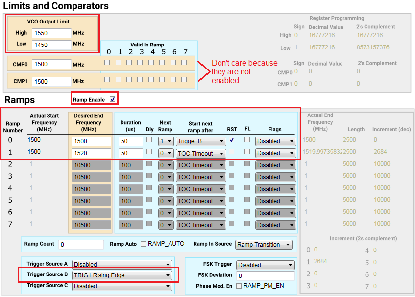 Figure 18. TICS Pro Ramp Calculator
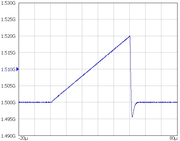 Figure 19. Single Sawtooth Ramp Example
8.2.6 Continuous Sawtooth Ramp Example
This example shows how to generate a continuous sawtooth ramp. Only one ramp segment is necessary as it will loop back to itself.
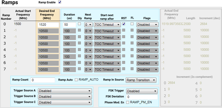 Figure 20. Continuous Sawtooth Ramp Configuration
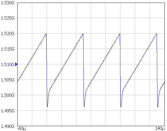 Figure 21. Continuous Sawtooth Ramp Example
8.2.7 Continuous Sawtooth Ramp with FSK Example
A ramp and FSK can coexist at the same time. Since the amount of FSK is added to the instantaneous carrier, the FSK will appear at the envelope of the ramp. Furthermore, a ramp and FSK are two independent operations, their register settings can be combined in a single configuration setting. That is, when RAMP_EN is enabled, both frequency ramp and FSK will be activated together.
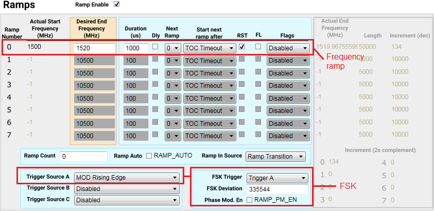 Figure 22. Continuous Sawtooth Ramp with FSK Configuration
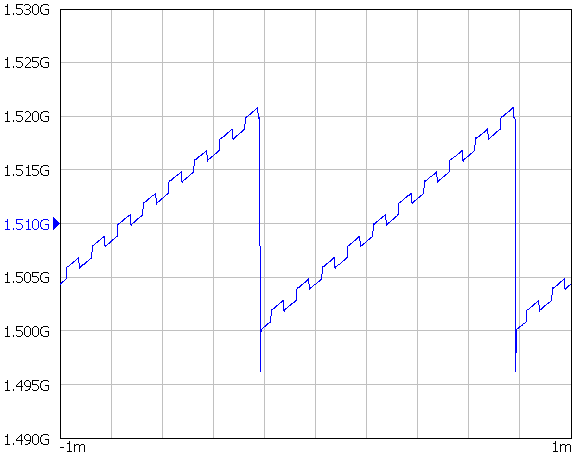 Figure 23. Continuous Sawtooth Ramp with FSK Example
8.2.8 Continuous Triangular Ramp Example
Two ramp segments are used to create this ramp pattern. RAMP0 ramps from 1500 MHz to 1520 MHz. RAMP1 brings the frequency back to 1500 MHz and then RAMP0 starts over again. Since RAMP1 already brought the frequency back to 1500 MHz, which is also the start frequency of RAMP0, a reset to fractional numerator is not required.
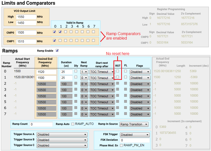 Figure 24. Continuous Triangular Ramp Configuration
Ramp comparators are enabled so as to output flag signals when the threshold frequencies are hit. MOD pin is assigned for CMP0 while TRIG1 pin is assigned for CMP1. RAMP_CMP0_EN is equal to 3 because ramp segment 0 and 1 are monitored.
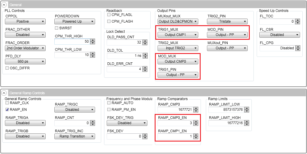 Figure 25. Ramp Comparators Configuration
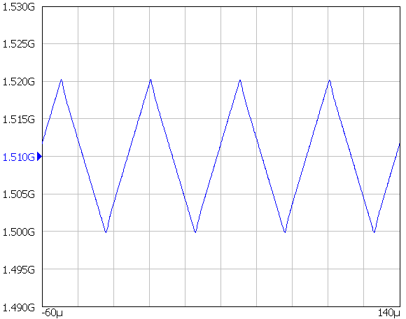 Figure 26. Continuous Triangular Ramp Example
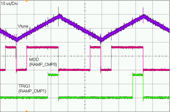 Figure 27. Ramp Comparators Output Flags
8.2.9 Continuous Trapezoid Ramp Example
This is a long-ramp example, the ramp duration is 2 ms. Since fPD = 50 MHz, 100000 ramps are required for each ramp segment. However, LMX2491 supports up to a maximum ramp length (RAMPx_LEN) of 65536 only. There are two solutions to resolve this problem:
- Reduce phase detector frequency. For example, reduce fPD to 25 MHz, then the required RAMPx_LEN becomes 50000.
- Enable RAMPx_DLY. When this register bit is set, the ramp generator will ramp every 2 phase detector cycles instead of the normal 1 fPD cycle. In this example, this bit is set and as a result, RAMPx_LEN is 50000.
Four ramp segments are used to construct the ramp pattern. Again there is no need to reset the fractional numerator because the last ramp end frequency is equal to the first ramp start frequency.
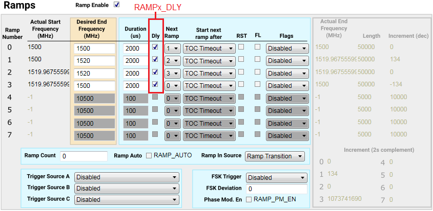 Figure 28. Continuous Trapezoid Ramp Configuration
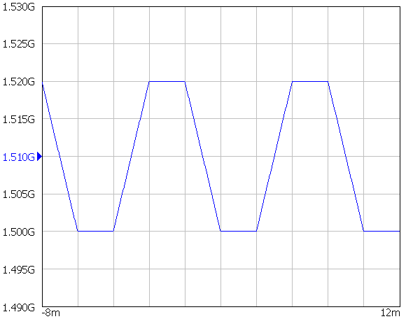 Figure 29. Continuous Trapezoid Ramp Example
8.2.10 Arbitrary Waveform Ramp Example
An arbitrary ramp waveform can be easily constructed with the 8 ramp segments provided in LMX2491. LMX2491 also provides flag signals output to indicate the start of a ramp. This example used the MOD pin to initiate the ramp and used TRIG1 and TRIG2 as the output flags to indicate the status of the ramp.
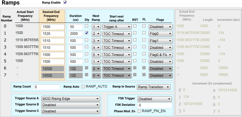 Figure 30. Arbitrary Waveform Ramp Configuration
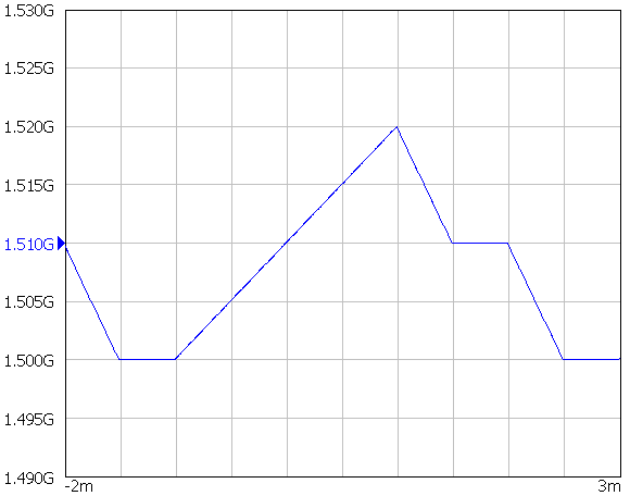 Figure 31. Arbitrary Waveform Ramp Example
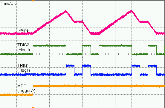 Figure 32. Arbitrary Waveform Ramp Timing