SNAS624B March   2014  – May 2015 LMX2492 , LMX2492-Q1

PRODUCTION DATA.  

  1. Features
  2. Applications
  3. Description
  4. Simplified Schematic
  5. Revision History
  6. Pin Configuration and Functions
  7. Specifications
    1. 7.1 Absolute Maximum Ratings
    2. 7.2 Storage Conditions
    3. 7.3 ESD Ratings
    4. 7.4 Recommended Operating Conditions
    5. 7.5 Thermal Information
    6. 7.6 Electrical Characteristics
    7. 7.7 Timing Requirements, Programming Interface (CLK, DATA, LE)
    8. 7.8 Typical Characteristics
  8. Detailed Description
    1. 8.1  Overview
    2. 8.2  Functional Block Diagram
    3. 8.3  Feature Description
      1. 8.3.1  OSCin Input
      2. 8.3.2  OSCin Doubler
      3. 8.3.3  R Divider
      4. 8.3.4  PLL N Divider
      5. 8.3.5  Fractional Circuitry
      6. 8.3.6  PLL Phase Detector and Charge Pump
      7. 8.3.7  External Loop Filter
      8. 8.3.8  Fastlock and Cycle Slip Reduction
      9. 8.3.9  Lock Detect and Charge Pump Voltage Monitor
        1. 8.3.9.1 Charge Pump Voltage Monitor
        2. 8.3.9.2 Digital Lock Detect
      10. 8.3.10 FSK/PSK Modulation
      11. 8.3.11 Ramping Functions
        1. 8.3.11.1 Ramp Count
        2. 8.3.11.2 Ramp Comparators and Ramp Limits
      12. 8.3.12 Power on Reset (POR)
    4. 8.4  Device Functional Modes
      1. 8.4.1 Continuous Frequency Generator
        1. 8.4.1.1 Integer Mode Operation
        2. 8.4.1.2 Fractional Mode Operation
      2. 8.4.2 Modulated Waveform Generator
    5. 8.5  Programming
      1. 8.5.1 Loading Registers
    6. 8.6  Register Map
    7. 8.7  Register Field Descriptions
      1. 8.7.1 POWERDOWN and Reset Fields
      2. 8.7.2 Dividers and Fractional Controls
        1. 8.7.2.1 Speed Up Controls (Cycle Slip Reduction and Fastlock)
    8. 8.8  Lock Detect and Charge Pump Monitoring
    9. 8.9  TRIG1,TRIG2,MOD, and MUXout Pins
    10. 8.10 Ramping Functions
    11. 8.11 Individual Ramp Controls
  9. Applications and Implementation
    1. 9.1 Application Information
    2. 9.2 Typical Applications
      1. 9.2.1 Design Requirements
      2. 9.2.2 Detailed Design Procedure
      3. 9.2.3 Application Performance Plot - Sawtooth Waveform Example
      4. 9.2.4 Application Performance Plot - Flat Top Triangle Waveform
      5. 9.2.5 Applications Performance Plot -- Complex Triggered Ramp
  10. 10Power Supply Recommendations
  11. 11Layout
    1. 11.1 Layout Guidelines
    2. 11.2 Layout Example
  12. 12Device and Documentation Support
    1. 12.1 Device Support
      1. 12.1.1 Development Support
    2. 12.2 Documentation Support
      1. 12.2.1 Related Documentation
    3. 12.3 Related Links
    4. 12.4 Community Resources
    5. 12.5 Trademarks
    6. 12.6 Electrostatic Discharge Caution
    7. 12.7 Glossary
  13. 13Mechanical, Packaging, and Orderable Information

パッケージ・オプション

メカニカル・データ(パッケージ|ピン)
サーマルパッド・メカニカル・データ
発注情報

11 Layout

11.1 Layout Guidelines

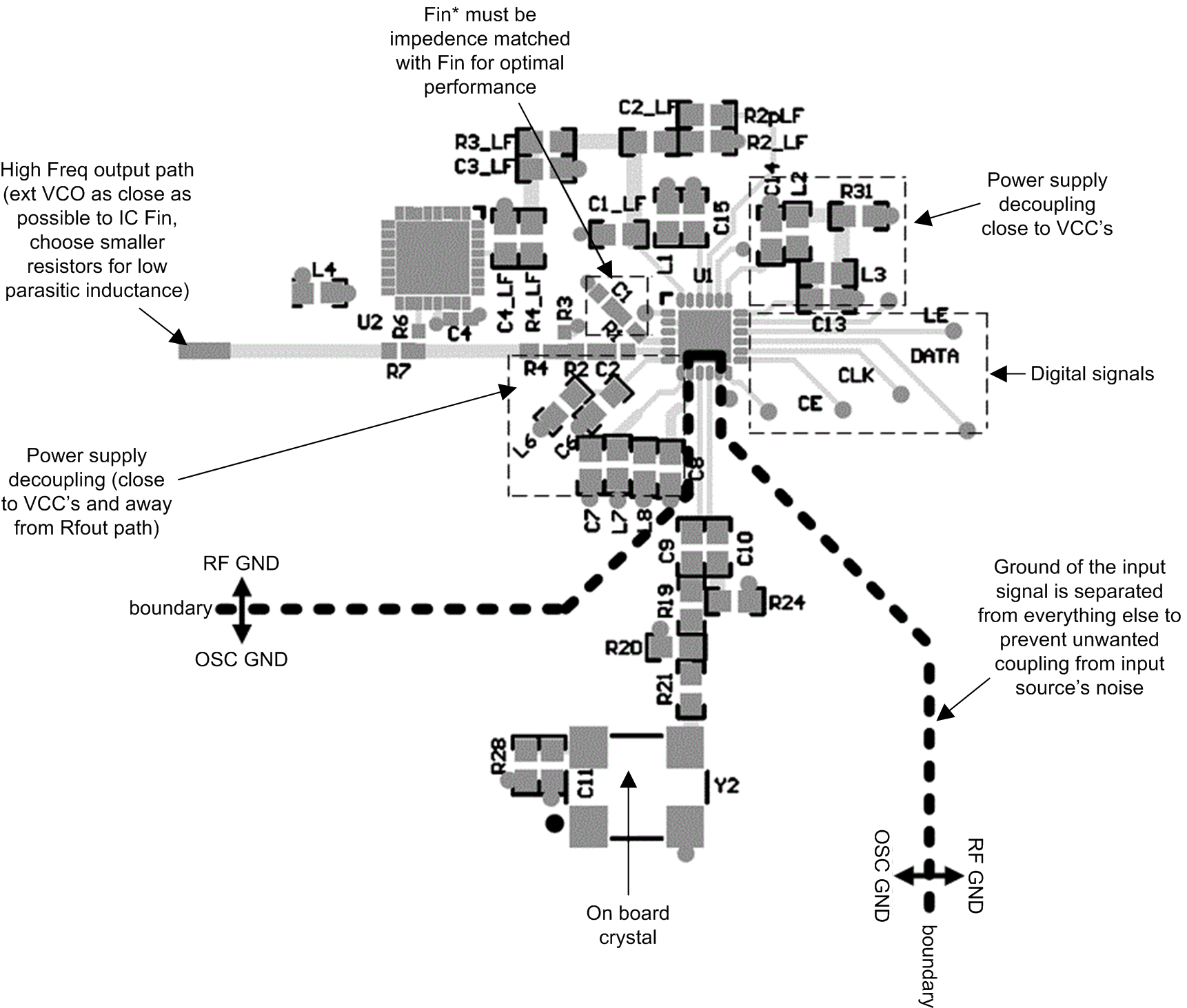
For layout examples, the EVM instructions are the most comprehensive document. In general, the layout guidelines are similar to most other PLL devices. For the high frequency Fin pin, it is recommended to use 0402 components and match the trace width to these pad sizes. Also the same needs to be done on the Fin* pin. If layout is easier to route the signal to Fin* instead of Fin, then this is acceptable as well.

11.2 Layout Example
LMX2492 LMX2492-Q1 pcb_snas624.png