SNOSB31J July 2009 – December 2014 LMX2541
PRODUCTION DATA.
- 1 Features
- 2 Applications
- 3 Description
- 4 Revision History
- 5 Device Comparison Table
- 6 Pin Configuration and Functions
- 7 Specifications
- 8 Parameter Measurement Information
-
9 Detailed Description
- 9.1 Overview
- 9.2 Functional Block Diagrams
- 9.3
Feature Description
- 9.3.1 PLL Reference Oscillator Input Pins
- 9.3.2 PLL R Divider
- 9.3.3 PLL Phase Detector and Charge Pump
- 9.3.4 PLL N Divider and Fractional Circuitry
- 9.3.5 Partially Integrated Loop Filter
- 9.3.6 Low Noise, Fully Integrated VCO
- 9.3.7 Programmable VCO Divider
- 9.3.8 Programmable RF Output Buffer
- 9.3.9 Powerdown Modes
- 9.3.10 Fastlock
- 9.3.11 Lock Detect
- 9.3.12 Current Consumption
- 9.3.13 Fractional Spurs
- 9.3.14 Impact of VCO_DIV on Fractional Spurs
- 9.3.15 PLL Phase Noise
- 9.3.16 Impact of Modulator Order, Dithering, and Larger Equivalent Fractions on Spurs and Phase Noise
- 9.3.17 Modulator Order
- 9.3.18 Programmable Output Power with On/Off
- 9.3.19 Loop Filter
- 9.3.20 Internal VCO Digital Calibration Time
- 9.4 Device Functional Modes
- 9.5 Programming
- 9.6
Register Maps
- 9.6.1
Register R7
- 9.6.1.1 Register R13
- 9.6.1.2 Register R12
- 9.6.1.3 Register R9
- 9.6.1.4 Register R8
- 9.6.1.5 Register R6
- 9.6.1.6 Register R5
- 9.6.1.7
Register R4
- 9.6.1.7.1 OSC_FREQ [7:0] -- OSCin Frequency for VCO Calibration Clocking
- 9.6.1.7.2 VCO_DIV[5:0] - VCO Divider
- 9.6.1.7.3 R3_LF[2:0] -- Value for Internal Loop Filter Resistor R3
- 9.6.1.7.4 R4_LF[2:0] -- Value for Internal Loop Filter Resistor R4
- 9.6.1.7.5 C3_LF[3:0] -- Value for C3 in the Internal Loop Filter
- 9.6.1.7.6 C4_LF[3:0] -- Value for C4 in the Internal Loop Filter
- 9.6.1.8
Register R3
- 9.6.1.8.1 MODE[1:0] -- Operational Mode
- 9.6.1.8.2 Powerdown -- Powerdown Bit
- 9.6.1.8.3 XO - Crystal Oscillator Mode Select
- 9.6.1.8.4 CPG[4:0] -- Charge Pump Current
- 9.6.1.8.5 MUX[3:0] -- Multiplexed Output for Ftest/LD Pin
- 9.6.1.8.6 CPP - Charge Pump Polarity
- 9.6.1.8.7 OSC2X-- OSCin Frequency Doubler
- 9.6.1.8.8 FDM - Extended Fractional Denominator Mode Enable
- 9.6.1.8.9 ORDER[2:0] -- Delta-Sigma Modulator Order
- 9.6.1.8.10 DITH[1:0] -- Dithering
- 9.6.1.8.11 CPT - Charge Pump TRI-STATE
- 9.6.1.8.12 DLOCK[2:0] - Controls for Digital Lock Detect
- 9.6.1.8.13 FSK - Frequency Shift Keying
- 9.6.1.9 Register R2
- 9.6.1.10 Registers R1 and R0
- 9.6.1
Register R7
-
10Application and Implementation
- 10.1
Application Information
- 10.1.1 Determining the Best Frequency Option of the LMX2541 to Use
- 10.1.2 RFout Output Power Test Setup
- 10.1.3 Phase Noise Measurement Test Setup
- 10.1.4 Input and Output Impedance Test Setup
- 10.1.5 ExtVCOin (NOT OSCin) Input Sensitivity Test Setup
- 10.1.6 OSCin Input Sensitivity Test Setup
- 10.1.7 Typical Connections
- 10.2 Typical Application
- 10.1
Application Information
- 11Power Supply Recommendations
- 12Layout
- 13Device and Documentation Support
- 14Mechanical, Packaging, and Orderable Information
パッケージ・オプション
デバイスごとのパッケージ図は、PDF版データシートをご参照ください。
メカニカル・データ(パッケージ|ピン)
- NJK|36
サーマルパッド・メカニカル・データ
発注情報
10 Application and Implementation
NOTE
Information in the following applications sections is not part of the TI component specification, and TI does not warrant its accuracy or completeness. TI’s customers are responsible for determining suitability of components for their purposes. Customers should validate and test their design implementation to confirm system functionality.
10.1 Application Information
10.1.1 Determining the Best Frequency Option of the LMX2541 to Use
When there are multiple devices that can satisfy the frequency requirement, performance characteristics can sometimes be used to make a decision. Consider the following example of where an output frequency of 1200 to 1250 MHz is desired with a channel spacing of 100 kHz. From the frequency table, the LMX2541SQ2380E could be used with a divide value of 2, or the LMX2541SQ3740E option could be used with a divide value of 3. This raises the question: Which one has better performance? The following table is helpful in comparing the performance.
| PERFORMANCE CHARACTERISTIC |
WHAT MAKES IT BETTER |
WHY |
|---|---|---|
| Fractional Spurs and Fraction Noise |
Larger Value of VCO_DIV | Fractional spurs at the VCO are independent of VCO frequency, but when the VCO frequency is divided down by a factor of VCO_DIV, the fractional spurs improve by a factor of 20·log(VCO_DIV). Also, the fractional channel spacing can be made wider at the VCO, which makes the fractional spurs farther from the carrier. The fractional noise of the modulator is divided down in a similar way as fractional spurs. In applications where this is dominant, this larger division can have an impact. Consult the applications section for more information on the fractional phase noise. |
| VCO Phase Noise | Operating in the lower frequency range of the VCO | At the lower end of the tuning range, the VCO phase noise is less because the tuning gain is less. This provides better phase noise, even accounting for the difference in frequency. |
Considering the fractional spurs and phase noise, the channel spacing at the 2380E VCO would be 200 kHz. When this is divided by two, the offset of these spurs does not change and the spurs at the VCO output would be reduced by a factor of 20·log(2) = 6 dB. The channel spacing at the 3740E VCO would be 300 kHz and these spurs would be reduced by a factor of 20·log(3) = 9.5 dB. So the spurs of the 3740E option would probably be better by virtue of the fact that they are farther from the carrier and easier to filter and also that they are divided down more by the VCO divider. The fractional phase noise would also be (9.5 - 6) = 3.5 dB better by the same reasoning.
Now consider the VCO phase noise. For the 3740E option, 1200 - 1250 MHz corresponds to a VCO frequency of 3600 - 3750 MHz, which is closer to the lower end of the tuning range for this device. For the 2380E option, this would correspond to 2400 - 2500 MHz, which is closer to the higher end of the tuning range. To verify this, take the phase noise numbers from the electrical specifications, extrapolate them to the actual frequencies, and then subtract a factor of 20·log(VCO_DIV). For the 2380E option, this works out to -116 dBc/Hz at 1200 MHz and -115.4 dBc/Hz at 1250 MHz. For the 3740E option, this works out to -117.4 dBc/Hz at 1200 MHz and -116.9 dBc/Hz at 1250 MHz.
10.1.2 RFout Output Power Test Setup
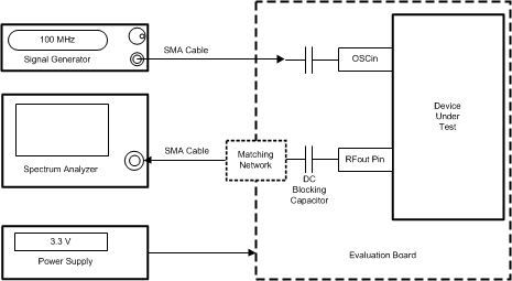
The output power is tested by programming the VCO output to a desired frequency and measuring with a spectrum analyzer. A 3 dB pad is used and this gain as well as any losses from the cable are added to the actual measurement. As for the DC blocking capacitor, typically 100 pF is used for frequencies above 2 GHz and 0.1 uF are used for frequencies below 2 GHz. It turns out that the measurement is not as sensitive as one would expect to this blocking capacitor value. The output power is mainly a function of the frequency of the output buffer and the settings of the VCO_DIV (1 or >1), OUTTERM, VCOGAIN, and DIVGAIN bits. It is not very sensitive to the actual frequency option of the part. For instance, the LMX2541SQ2060E and the LMX2541SQ2380E both should have similar output power at 2.2 GHz. Note that this same test setup can also be used to measure harmonics.
10.1.3 Phase Noise Measurement Test Setup
The basic setup technique for all noise tests is to measure the noise at the output of the RFout pin in Internal VCO Mode (MODE=0) with a phase noise analyzer. For all measurements, the internal loop filter components (LF_R3, LF_R4, LF_C3, and LF_C4) should be set to their minimum values. There are some special considerations depending on what kind of noise is being measured.
10.1.3.1 PLL Phase Noise Measurement
To get an accurate measurement of the PLL phase noise, one needs to ensure four things.
- The PLL loop bandwidth is sufficiently wide so that the VCO noise does not degrade the measurement
- The measurement is not corrupted by peaking in the loop filter response.
- The reference source is sufficiently clean so that this does not degrade the measurement.
- A distinction is made between the PLL flat noise and the PLL 1/f noise
If the PLL loop bandwidth is made as wide as possible, then this helps keep the peaking of the loop filter response and the VCO noise from degrading the measurement. For the ultimate accuracy, this loop filter response can be factored into the measurement. As for the cleanliness of the reference source, the best sources tend to be those that are fixed, such as a 100 MHz Wenzel oscillator. Signal generators tend to be noisy, but if that is all that is available, then there are a few things that can help compensate for this. One technique is to use a higher frequency and divide this down to a lower frequency. For instance, a 500 MHz signal divided down to 20 MHz typically has much better phase noise than a direct 20 MHz signal, if it comes from a signal generator. Another technique is to measure the noise of the reference source and then multiply it up and then subtract it from the measurement. For instance, if the signal source was 500 MHz and the output frequency was 4 GHz, this signal source noise would be multiplied up by a factor of 20·log(4 GHz / 500 MHz) = 18 dB. Once that is done, the 1/f noise and the flat noise can be measured.
10.1.3.1.1 PLL Phase Noise Measurement - 1/f Noise
The 1/f noise dominates closer to the carrier. Special care should be taken to ensure that this is not the noise of the reference source. The noise contribution of the reference source at the RFout pin can be calculating by measuring what is coming into the OSCin pin and then adding a correction factor of 20·log( fRFout / fOSCin) . A characteristic of this noise is that it follows a 10 dB/decade slope. If the slope of the measured noise looks more than 10 dB/decade, it is likely to be the reference source, not the LMX2541 device. Another characteristic of the 1/f noise is that it is independent of phase detector frequency. So to fully expose the 1/f noise, raise the phase detector frequency as high as possible, because this lowers the flat noise, but not the 1/f noise.
10.1.3.1.2 PLL Phase Noise Measurement - Flat Noise
The PLL flat noise is measured at an offset that is not too close to the PLL 1/f noise, but also well inside the loop bandwidth. Many phase noise profiles have a point where the PLL noise flattens to a minimum value between the carrier and the loop bandwidth. This is where the flat noise should be measured. To measure the 1 Hz normalized phase noise, it is often easier to measure this with a lower phase detector frequency so that this flat noise is higher and easier to measure.
10.1.3.2 VCO Phase Noise Measurement
In order to measure the VCO phase noise, the loop filter resistors should be set to their minimum value to reduce their noise contribution. The loop bandwidth should also be made as narrow as possible. Because the loop bandwidth is very narrow, the cleanliness of the OSCin signal is therefore not as important. The phase noise is measured outside the loop bandwidth of the system.
An alternative way that might not be as accurate, but is much easier to do is to lock the device to a frequency and then set the CPT bit to 1 to disable the charge pump. The VCO will drift a little, the averaging on the equipment should be reset after this bit is changed and one cannot take to long to take this measurement. Test equipment that tracks the signal source is better if using this open loop technique.
10.1.3.3 Divider Phase Noise Measurement
The basic method for measuring the divider noise is to drive the divider with a noise source of known value and then subtract away this noise. The divider noise floor tends to be flat, whereas the VCO phase noise decreases with offset frequency, so this measurement is made at as far of an offset that is possible. When using Internal VCO Mode (MODE=0), the raw VCO phase noise with VCO_DIV=1 can be measured. Then the VCO divider can be programmed to get close to the desired frequency. For example, the VCO frequency can be set to 4 GHz and the phase noise measured. This phase noise data can be saved or downloaded. Suppose then that one was interested in the divider noise at 400 MHz. The VCO divider could be set to 10 and then 20 dB is subtracted from the VCO phase noise to figure its contribution at 400 MHz. Provided that the actual phase noise measured at 400 MHz with VCO_DIV is above this, then one can assume that this is the noise of the divider.
An alternative way to measure this is to drive the OSCin pin and use Divider Only (MODE=2) to measure the phase noise. This gives direct control of the frequency, but one should be sure that the noise being measured is the device and not the frequency source.
10.1.4 Input and Output Impedance Test Setup
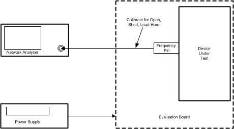
A network analyzer can be used to measure the input impedance of the OSCin and ExtVCOin pin as well as the output impedance of the RFout pin. The general technique is to connect the desired pin with no DC blocking capacitor to a network analyzer and measure the impedance directly. The part needs to be programmed to ensure that it is in a known state. There are some special considerations that should be taken for different measurements of the three different impedances.
10.1.4.1 OSCin Input Impedance Measurement
For this pin, the provided calibration standards are typically good enough for a decent measurement. A single-ended measurement at the OSCin or OSCin* pins can be made For a differential measurement, this needs to be treated by the instrument as a two port network.
10.1.4.2 ExtVCOin Input Impedance Measurement
Because this pin goes higher in frequency, it is often difficult get a good measurement at higher frequencies because of the effects of the board and SMA connector. One technique that can be used is instead of using the provided calibration standards that come with the equipment, solder resistors directly to the board in order to calibrate out the effects of the board as well. A 0 ohm resistor functions as a short, no resistor functions as an open, and two parallel 100 ohm resistors serve as a load. These should be soldered as close to the part as possible. Once this calibration is done, the measurement can be done as normal.
10.1.4.3 RFout Output Impedance Measurement
Although output and input impedance are not the same thing, they can be measured in a similar way. Because this pin is a higher frequency, it is better to use the same method for calibration as used for the ExtVCOin pin. The other consideration for the RFout pin is that there are many different settings that impact this input impedance. When in bypass mode (VCO_DIV=1), the VCOGAIN and OUTTERM words can change the impedance. When in divided mode (VCO_DIV>1), the DIVGAIN and OUTTERM words can impact the impedance.
10.1.5 ExtVCOin (NOT OSCin) Input Sensitivity Test Setup
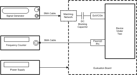
In order to measure the ExtVCOin Input sensitivity, the part is put in External VCO mode and a signal is applied to the ExtVCOin pin. A matching network, which is typically a 3 dB pad, is used and this loss is added to the measured numbers as well as any potential cable losses (on the order of 1 dB). A signal is applied at a known frequency and power and the output of the N counter is monitored using the Ftest/LD pin and setting it to look at the N counter output divided by 2. Typically, the divide by 2 function is better because if it is not used, the duty cycle from the Ftest/LD pin is not 50% and this can sometimes confuse frequency counters. The part is set in fractional mode with a large fraction of 502 + 2097150/4194301 to ensure that the fractional circuitry gets fully tested. Accounting for the extra divide by 2 from the Ftest/LD pin, the divided output frequency should be the input frequency divided by 1005 to a 1 ppm tolerance.
10.1.6 OSCin Input Sensitivity Test Setup
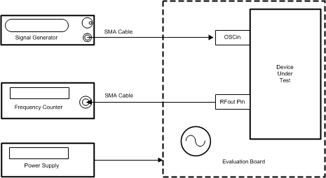
10.1.6.1 Input Sensitivity Test Procedure
There are two things that are important to consider when measuring the OSCin sensitivity.
- The action of setting the Ftest/LD pin to monitor the R divider output degrades the OSCin sensitivity.
- The internal VCO frequency calibration is based on the OSCin signal
Because of these considerations, the OSCin sensitivity needs to be measured in a closed loop test in such a way that the internal frequency calibration is not distorting the measurement. To do this, a known frequency and power level are set at the OSCin pin and the power level is changed until the PLL becomes more than 1 ppm off frequency. The PLL_R divider is varied to maintain a phase detector frequency of 1 MHz to ensure that the PLL loop does not become unstable. The frequency counter needs to be synchronized in frequency to the signal generator. It is better to use a narrower loop bandwidth for this test because the phase noise of the PLL might degrade when the OSCin power level gets to close to the sensitivity limits. Typically, a 0.1 uF capacitor is used as a DC block for the signal at the OSCin pin. The sensitivity at the OSCin pin is measured with a single-ended input.
This test can be run in internal VCO mode (MODE=0) or external VCO mode (MODE=1). When doing the test in internal VCO mode, the part needs to be initially locked and then the R counter is programmed to adjust for the OSCin frequency. However, in internal VCO mode, the PLL_N counter cannot be programmed, because the action of programming this counter activates the internal VCO frequecy calibration, which can interfere with the test.
10.1.6.2 OSCin Slew Rate Tests
There are two methods that can be used to test the OSCin slew rate. One method is to use test equipment that actually allows the user to vary the slew rate directly, but this type of equipment typically does not give the user enough range of adjustability. Another method is to calculate the slew rate based on the slope of a sine wave of known frequency and amplitude. For this method, the slew rate can be calculated from the frequency and peak to peak amplitude of the OSCin signal as follows: SlewOSCin = 2 × π × fOSCin × VppOSCin
10.1.7 Typical Connections
10.1.7.1 Full Chip Mode, Differential OSCin

10.1.7.2 External VCO Mode, Single-Ended OSCin, RFout Pin not Used

For both of the able connection diagrams, L1, L2, and Lmid should be left open, but the pads should be placed on these pins for optimal solderability. The GND pins should have separate vias to ground and the GND DAP also needs to be grounded with 9 vias. The VccVCO, VccRFout, and VccDiv pins can be shorted to the power plane, but need to be connected. For the other Vcc pins, ferrite beads and bypass capacitors may be added in order to improve spurious performance. VregVCO and VrefVCO need to be connected even if the internal VCO is not being used. The VregRFout pin only needs to be connected if the RFout pin is being used. When a block is not used, it is always still necessary to connect the corresponding Vcc pin, but the bypassing is not necessary, as shown in the above diagram for the external VCO mode.
10.1.7.3 OSCin/OSCin* Connections
For single-ended operation, the signal is driven into the OSCin pin. The OSCin* pin is terminated the same as the OSCin pin. This is a typical case if the device is driven by a TCXO. For both single-ended and differential operation, the input is AC coupled because the OSCin/OSCin* pins self-bias to an optimal DC operating point. Better performance for both phase noise and fractional spurs is obtained for signals with a higher slew rate, such as a square wave. This is especially important for lower frequency signals, because slower frequency sine waves have lower slew rates. Fractional spurs are typically about four dB better when running in differential mode as opposed to single-ended mode.
10.1.7.3.1 Single-Ended Operation

For differential operation, as is the case when using an LVDS or LVPECL driver, a 100 Ω resistor is placed across the OSCin/OSCin* traces
10.1.7.3.2 Differential Operation

A third way to configure the device is in crystal mode (XO = 1). For this, the crystal is placed across the OSCin/OSCin* pins. Crystals are specified for a specific load capacitance, CLoad. The load capacitors shown in the figure each have a value of CLoad/2.
10.1.7.3.3 Crystal Mode Operation

10.2 Typical Application

10.2.1 Design Requirements
Consider generating 4000.25 MHz from a 100-MHz XO input frequency.
For this design example, use the parameters listed in Table 19 as the user-input parameters.
Table 19. Design Parameters
| PARAMETER | VALUE | REASON FOR CHOOSING |
|---|---|---|
| Fout | 4000.25 MHz | This parameter was given. |
| Fosc | 100 MHz | This parameter was given. |
| Fpd | 25 MHz | Although the phase detector could be chosen to be 100 MHz, it is being chosen lower to reduce the integer boundary spur at 250 kHz offset. |
| Loop Bandwidth | 53 kHz | A wider bandwidth gives better in-band phase noise, but then the integer boundary spur is higher. This gives a reasonable trade-off. |
| Kpd | 3.2 mA | Maximum charge pump gain is best for the lowest PLL phase noise. |
| C1_LF | 2.2 nF | The external loop filter components can be found using design software from TI. |
| C2_LF | 22 nF | |
| R2_LF | 470 Ω | |
| C3_LF | 20 pF | The internal loop filter was chosen with the resistors to a lower setting to allow a wider bandwidth. However, it is best to put the most capacitance on C4 as it gives more filtering. |
| C4_LF | 100 pF | |
| R3_LF | 1 kΩ | |
| R4_LF | 200 Ω |
10.2.2 Detailed Design Procedure
Use the WEBENCH® Clock Architect to calculate the values of C2_LF and R2_LF.
Use C4 for the largest capacitance because it offers more filtering.
10.2.3 Application Curves
For Figure 30 and Figure 31, a third order modulator with dithering disabled was used with a fractional denominator of 500000. The charge pump gain was 32X and the loop filter components were C1 = 2.2 nF, C2 = 22 nF, R2 = 470 Ω. The internal loop filter components were C3_LF = 20 pF, C4_LF = 100 pF, R3_LF = 1 kΩ, R4_LF = 200 Ω.


 Figure 33. Phase Noise at 4000.25 MHz

")
(VCO Relocked at Each Temperature Vcc = 3.3 V, AC_TEMP_COMP = 5)
 Figure 34. Integer Boundary Spur Measurement