JAJSFM8B June 2018 – May 2019 LMZM33606
PRODUCTION DATA.
- 1 特長
- 2 アプリケーション
- 3 概要
- 4 改訂履歴
- 5 Pin Configuration and Functions
- 6 Specifications
-
7 Detailed Description
- 7.1 Overview
- 7.2 Functional Block Diagram
- 7.3
Feature Description
- 7.3.1 Adjusting the Output Voltage
- 7.3.2 Input Capacitor Selection
- 7.3.3 Output Capacitor Selection
- 7.3.4 Transient Response
- 7.3.5 Feed-Forward Capacitor
- 7.3.6 Switching Frequency (RT)
- 7.3.7 Synchronization (SYNC/MODE)
- 7.3.8 Output Enable (EN)
- 7.3.9 Programmable System UVLO (EN)
- 7.3.10 Internal LDO and BIAS_SEL
- 7.3.11 Power Good (PGOOD) and Power Good Pull-Up (PGOOD_PU)
- 7.3.12 Mode Select (Auto or FPWM)
- 7.3.13 Soft Start and Voltage Tracking
- 7.3.14 Voltage Dropout
- 7.3.15 Overcurrent Protection (OCP)
- 7.3.16 Thermal Shutdown
- 7.4 Device Functional Modes
- 8 Application and Implementation
- 9 Power Supply Recommendations
- 10Layout
- 11デバイスおよびドキュメントのサポート
- 12メカニカル、パッケージ、および注文情報
パッケージ・オプション
デバイスごとのパッケージ図は、PDF版データシートをご参照ください。
メカニカル・データ(パッケージ|ピン)
- RLX|41
サーマルパッド・メカニカル・データ
発注情報
7.3.14 Voltage Dropout
Voltage dropout is the minimum difference between the input voltage and output voltage that is required to maintain output voltage regulation while providing the rated output current.
To ensure the LMZM33606 maintains output voltage regulation at the recommended switching frequency, over the operating temperature range, the following requirements apply:
For output voltages ≤ 5 V, the minimum VIN is 3.5 V or (VOUT + 1 V), whichever is greater.
For output voltages > 5 V, the minimum VIN is (1.1 × VOUT).
space
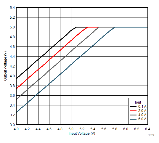
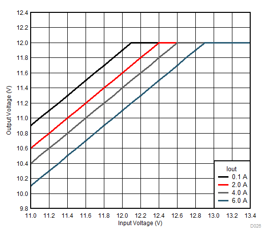
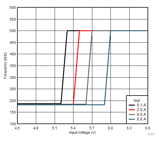
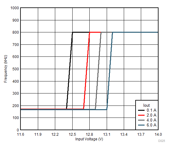
However, if fixed switching frequency operation is not required, the LMZM33606 operates in a frequency foldback mode when the dropout voltage is less than the recommendations above. Frequency foldback reduces the switching frequency to allow the output voltage to maintain regulation as input voltage decreases. Figure 41 through Figure 44 show typical dropout voltage and frequency foldback curves for 5 V and 12 V outputs at TA = 25°C. (As ambient temperature increases, dropout voltage and frequency foldback occur at higher input voltages.)
| VOUT = 5 V | fSW = 500 kHz |

| VOUT = 12 V | fSW = 800 kHz |

| VOUT = 5 V | fSW = 500 kHz |

| VOUT = 12 V | fSW = 800 kHz |