SNOSB14D August 2009 – December 2014 LPV521
PRODUCTION DATA.
- 1 Features
- 2 Applications
- 3 Description
- 4 Revision History
- 5 Pin Configuration and Functions
-
6 Specifications
- 6.1 Absolute Maximum Ratings
- 6.2 ESD Ratings
- 6.3 Recommended Operating Conditions
- 6.4 Thermal Information
- 6.5 1.8-V DC Electrical Characteristics
- 6.6 1.8-V AC Electrical Characteristics
- 6.7 3.3-V DC Electrical Characteristics
- 6.8 3.3-V AC Electrical Characteristics
- 6.9 5-V DC Electrical Characteristics
- 6.10 5-V AC Electrical Characteristics
- 6.11 Typical Characteristics
- 7 Detailed Description
- 8 Applications and Implementation
- 9 Power Supply Recommendations
- 10Layout
- 11Device and Documentation Support
- 12Mechanical, Packaging, and Orderable Information
7 Detailed Description
7.1 Overview
The LPV521 is fabricated with Texas Instruments' state-of-the-art VIP50 process. This proprietary process dramatically improves the performance of Texas Instruments' low-power and low-voltage operational amplifiers. The following sections showcase the advantages of the VIP50 process and highlight circuits which enable ultra-low power consumption.
7.2 Functional Block Diagram
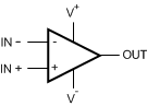 Figure 61. Block Diagram
7.3 Feature Description
The amplifier's differential inputs consist of a noninverting input (+IN) and an inverting input (–IN). The amplifier amplifies only the difference in voltage between the two inputs, which is called the differential input voltage. The output voltage of the op-amp Vout is given by Equation 1:
where AOL is the open-loop gain of the amplifier, typically around 100 dB (100,000x, or 10uV per Volt).
7.4 Device Functional Modes
7.4.1 Input Stage
The LPV521 has a rail-to-rail input which provides more flexibility for the system designer. Rail-to-rail input is achieved by using in parallel, one PMOS differential pair and one NMOS differential pair. When the common mode input voltage (VCM) is near V+, the NMOS pair is on and the PMOS pair is off. When VCM is near V−, the NMOS pair is off and the PMOS pair is on. When VCM is between V+ and V−, internal logic decides how much current each differential pair will get. This special logic ensures stable and low distortion amplifier operation within the entire common mode voltage range.
Because both input stages have their own offset voltage (VOS) characteristic, the offset voltage of the LPV521 becomes a function of VCM. VOS has a crossover point at 1.0 V below V+. Refer to the ’VOS vs. VCM’ curve in the Typical Performance Characteristics section. Caution should be taken in situations where the input signal amplitude is comparable to the VOS value and/or the design requires high accuracy. In these situations, it is necessary for the input signal to avoid the crossover point. In addition, parameters such as PSRR and CMRR which involve the input offset voltage will also be affected by changes in VCM across the differential pair transition region.
7.4.2 Output Stage
The LPV521 output voltage swings 3 mV from rails at 3.3-V supply, which provides the maximum possible dynamic range at the output. This is particularly important when operating on low supply voltages.
The LPV521 Maximum Output Voltage Swing defines the maximum swing possible under a particular output load. The LPV521 output swings 50 mV from the rail at 5-V supply with an output load of 100 kΩ.