JAJSFL3B November 2010 – June 2018 MSP430AFE221 , MSP430AFE222 , MSP430AFE223 , MSP430AFE231 , MSP430AFE232 , MSP430AFE233 , MSP430AFE251 , MSP430AFE252 , MSP430AFE253
PRODUCTION DATA.
- 1デバイスの概要
- 2改訂履歴
- 3Device Comparison
- 4Terminal Configuration and Functions
-
5Specifications
- 5.1 Absolute Maximum Ratings
- 5.2 ESD Ratings
- 5.3 Recommended Operating Conditions
- 5.4 Thermal Resistance Characteristics for PW-24 Package
- 5.5 Active Mode Supply Current (Into DVCC and AVCC) Excluding External Current
- 5.6 Typical Characteristics – Active-Mode Supply Current (Into DVCC and AVCC)
- 5.7 Low-Power-Mode Supply Currents (Into VCC) Excluding External Current
- 5.8 Typical Characteristics – LPM4 Current
- 5.9 Schmitt-Trigger Inputs (Ports Px and RST/NMI)
- 5.10 Leakage Current (Ports Px)
- 5.11 Outputs (Ports Px)
- 5.12 Output Frequency (Ports Px)
- 5.13 Typical Characteristics – Outputs
- 5.14 POR, BOR
- 5.15 Typical Characteristics – POR, BOR
- 5.16 Supply Voltage Supervisor (SVS), Supply Voltage Monitor (SVM)
- 5.17 Main DCO Characteristics
- 5.18 DCO Frequency
- 5.19 Calibrated DCO Frequencies – Tolerance
- 5.20 Wake-up Times From Lower-Power Modes (LPM3, LPM4)
- 5.21 Typical Characteristics – DCO Clock Wake-up Time
- 5.22 Internal Very-Low-Power Low-Frequency Oscillator (VLO)
- 5.23 Crystal Oscillator (XT2)
- 5.24 Typical Characteristics – XT2 Oscillator
- 5.25 SD24_A, Power Supply
- 5.26 SD24_A, Input Range
- 5.27 SD24_A, Performance
- 5.28 SD24_A, Temperature Sensor and Built-In VCC Sense
- 5.29 SD24_A, Built-In Voltage Reference
- 5.30 SD24_A, Reference Output Buffer
- 5.31 SD24_A, External Reference Input
- 5.32 USART0
- 5.33 Timer_A3
- 5.34 Flash Memory
- 5.35 RAM
- 5.36 JTAG and Spy-Bi-Wire Interface
- 5.37 JTAG Fuse
-
6Detailed Description
- 6.1 CPU
- 6.2 Instruction Set
- 6.3 Operating Modes
- 6.4 Interrupt Vector Addresses
- 6.5 Special Function Registers
- 6.6 Memory Organization
- 6.7 Flash Memory
- 6.8 Peripherals
- 6.9 Oscillator and System Clock
- 6.10 Brownout, Supply Voltage Supervisor
- 6.11 Digital I/O
- 6.12 Watchdog Timer (WDT+)
- 6.13 Timer_A3
- 6.14 USART0
- 6.15 Hardware Multiplier
- 6.16 SD24_A
- 6.17 Peripheral File Map
- 6.18
I/O Port Schematics
- 6.18.1 Port P1 Pin Schematic: P1.0 Input/Output With Schmitt Trigger
- 6.18.2 Port P1 Pin Schematic: P1.1 and P1.2 Input/Output With Schmitt Trigger
- 6.18.3 Port P1 Pin Schematic: P1.3 Input/Output With Schmitt Trigger
- 6.18.4 Port P1 Pin Schematic: P1.4 Input/Output With Schmitt Trigger
- 6.18.5 Port P1 Pin Schematic: P1.5 to P1.7 Input/Output With Schmitt Trigger
- 6.18.6 Port P2 Pin Schematic: P2.0 Input/Output With Schmitt Trigger
- 6.18.7 Port P2 Pin Schematic: P2.6, Input/Output With Schmitt Trigger
- 6.18.8 Port P2 Pin Schematic: P2.7, Input/Output With Schmitt Trigger
- 6.18.9 JTAG Fuse Check Mode
- 7デバイスおよびドキュメントのサポート
- 8メカニカル、パッケージ、および注文情報
5.16 Supply Voltage Supervisor (SVS), Supply Voltage Monitor (SVM)(3)
over recommended ranges of supply voltage and operating free-air temperature (unless otherwise noted)| PARAMETER | TEST CONDITIONS | MIN | TYP | MAX | UNIT | |
|---|---|---|---|---|---|---|
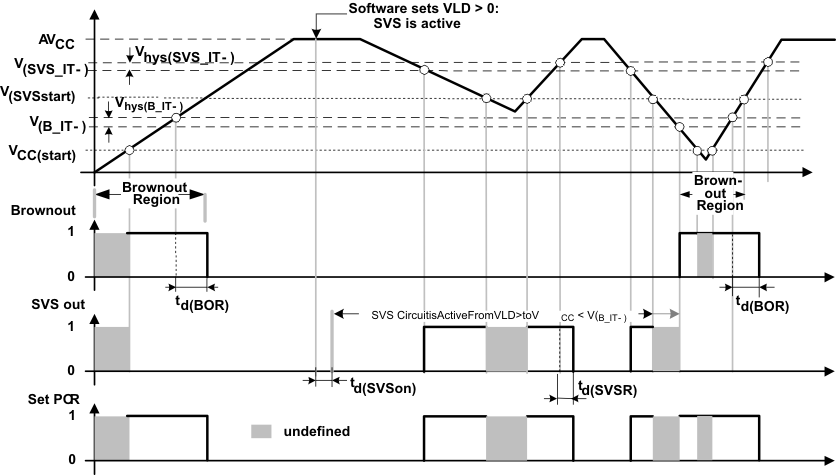
| t(SVSR) | dVCC/dt > 30 V/ms (see Figure 5-12) | 100 | µs | |||
| dVCC/dt ≤ 30 V/ms | 2000 | |||||
| td(SVSon) | SVS on, switch from VLD = 0 to VLD ≠ 0, VCC =3 V | 100 | µs | |||
| tsettle | VLD ≠ 0(2) | 12 | µs | |||
| V(SVSstart) | VLD ≠ 0, VCC/dt ≤ 3 V/s (see Figure 5-12) | 1.55 | 1.7 | V | ||
| Vhys(SVS_IT-) | VCC/dt ≤ 3 V/s (see Figure 5-12) | VLD = 1 | 120 | mV | ||
| VLD = 2 to 14 | 15 | |||||
| VCC/dt ≤ 3 V/s (see Figure 5-12), external voltage applied on SVSIN | VLD = 15 | 10 | ||||
| V(SVS_IT-) | VCC/dt ≤ 3V/s (see Figure 5-12) | VLD = 1 | 1.8 | 1.9 | 2.05 | V |
| VLD = 2 | 2.1 | |||||
| VLD = 3 | 2.2 | |||||
| VLD = 4 | 2.3 | |||||
| VLD = 5 | 2.24 | 2.4 | 2.6 | |||
| VLD = 6 | 2.5 | |||||
| VLD = 7 | 2.65 | |||||
| VLD = 8 | 2.8 | |||||
| VLD = 9 | 2.69 | 2.9 | 3.13 | |||
| VLD = 10 | 3.05 | |||||
| VLD = 11 | 3.2 | |||||
| VLD = 12 | 3.35 | |||||
| VLD = 13 | 3.24 | 3.5 | 3.76(1) | |||
| VLD = 14 | 3.7(1) | |||||
| VCC/dt ≤ 3 V/s (see Figure 5-12), external voltage applied on SVSIN | VLD = 15 | 1.1 | 1.2 | 1.3 | ||
| ICC(SVS)(3) | VLD ≠ 0, VCC = 3 V | 12 | 17 | µA | ||
(1) The recommended operating voltage range is limited to 3.6 V.
(2) tsettle is the settling time that the comparator operational amplifier needs to have a stable level after VLD is switched from VLD ≠ 0 to a different VLD value between 2 and 15. The overdrive is assumed to be greater than 50 mV.
(3) The current consumption of the SVS module is not included in the ICC current consumption data.
 Figure 5-12 SVS Reset (SVSR) vs Supply Voltage
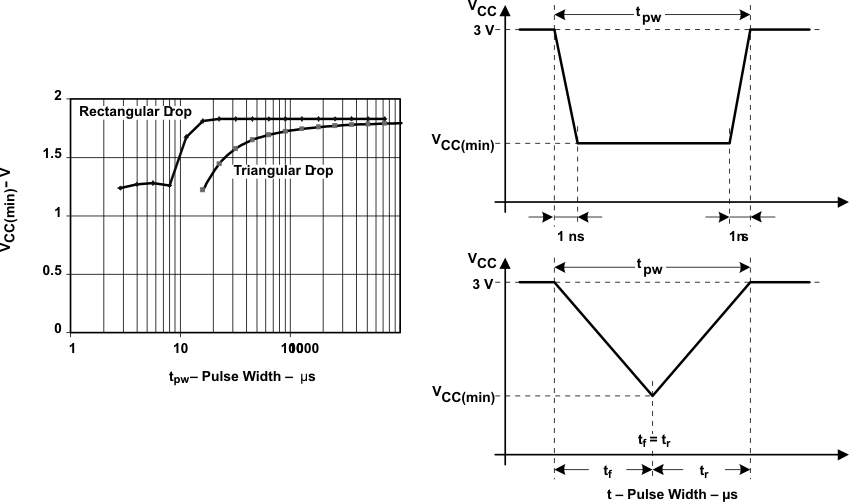
  Figure 5-13 VCC(min) With a Square Voltage Drop and a Triangular Voltage Drop to Generate an SVS Signal