SLVSCN6A November 2014 – December 2014 MSP430FR5739-EP
PRODUCTION DATA.
- 1Device Overview
- 2Revision History
- 3Pin Configuration and Functions
-
4Specifications
- 4.1 Absolute Maximum Ratings
- 4.2 Recommended Operating Conditions
- 4.3 Thermal Information
- 4.4 Active Mode Supply Current Into VCC Excluding External Current
- 4.5 Low-Power Mode Supply Currents (Into VCC) Excluding External Current
- 4.6 Schmitt-Trigger Inputs - General Purpose I/O (P1.0 to P1.7, P2.0 to P2.7, P3.0 to P3.7, P4.0 to P4.1, PJ.0 to PJ.5, RST/NMI)
- 4.7 Inputs - Ports P1 and P2 (P1.0 to P1.7, P2.0 to P2.7)
- 4.8 Leakage Current - General Purpose I/O (P1.0 to P1.7, P2.0 to P2.7, P3.0 to P3.7, P4.0 to P4.1, PJ.0 to PJ.5, RST/NMI)
- 4.9 Outputs - General Purpose I/O (P1.0 to P1.7, P2.0 to P2.7, P3.0 to P3.7, P4.0 to P4.1, PJ.0 to PJ.5)
- 4.10 Output Frequency - General Purpose I/O (P1.0 to P1.7, P2.0 to P2.7, P3.0 to P3.7, P4.0 to P4.1, PJ.0 to PJ.5)
- 4.11 Typical Characteristics - Outputs
- 4.12 Crystal Oscillator, XT1, Low-Frequency (LF) Mode
- 4.13 Crystal Oscillator, XT1, High-Frequency (HF) Mode
- 4.14 Internal Very-Low-Power Low-Frequency Oscillator (VLO)
- 4.15 DCO Frequencies
- 4.16 MODOSC
- 4.17 PMM, Core Voltage
- 4.18 PMM, SVS, BOR
- 4.19 Wake-Up from Low Power Modes
- 4.20 Timer_A
- 4.21 Timer_B
- 4.22 eUSCI (UART Mode) Recommended Operating Conditions
- 4.23 eUSCI (UART Mode)
- 4.24 eUSCI (SPI Master Mode) Recommended Operating Conditions
- 4.25 eUSCI (SPI Master Mode)
- 4.26 eUSCI (SPI Slave Mode)
- 4.27 eUSCI (I2C Mode)
- 4.28 10-Bit ADC, Power Supply and Input Range Conditions
- 4.29 10-Bit ADC, Timing Parameters
- 4.30 10-Bit ADC, Linearity Parameters
- 4.31 REF, External Reference
- 4.32 REF, Built-In Reference
- 4.33 REF, Temperature Sensor and Built-In VMID
- 4.34 Comparator_D
- 4.35 FRAM
- 4.36 JTAG and Spy-Bi-Wire Interface
-
5Detailed Description
- 5.1 Functional Block Diagram
- 5.2 CPU
- 5.3 Operating Modes
- 5.4 Interrupt Vector Addresses
- 5.5 Memory Organization
- 5.6 Bootstrap Loader (BSL)
- 5.7 JTAG Operation
- 5.8 FRAM
- 5.9 Memory Protection Unit (MPU)
- 5.10
Peripherals
- 5.10.1 Digital I/O
- 5.10.2 Oscillator and Clock System (CS)
- 5.10.3 Power Management Module (PMM)
- 5.10.4 Hardware Multiplier (MPY)
- 5.10.5 Real-Time Clock (RTC_B)
- 5.10.6 Watchdog Timer (WDT_A)
- 5.10.7 System Module (SYS)
- 5.10.8 DMA Controller
- 5.10.9 Enhanced Universal Serial Communication Interface (eUSCI)
- 5.10.10 TA0, TA1
- 5.10.11 TB0, TB1, TB2
- 5.10.12 ADC10_B
- 5.10.13 Comparator_D
- 5.10.14 CRC16
- 5.10.15 Shared Reference (REF)
- 5.10.16 Embedded Emulation Module (EEM)
- 5.10.17 Peripheral File Map
-
6Input/Output Schematics
- 6.1 Port P1, P1.0 to P1.2, Input/Output With Schmitt Trigger
- 6.2 Port P1, P1.3 to P1.5, Input/Output With Schmitt Trigger
- 6.3 Port P1, P1.6 to P1.7, Input/Output With Schmitt Trigger
- 6.4 Port P2, P2.0 to P2.2, Input/Output With Schmitt Trigger
- 6.5 Port P2, P2.3 to P2.4, Input/Output With Schmitt Trigger
- 6.6 Port P2, P2.5 to P2.6, Input/Output With Schmitt Trigger
- 6.7 Port P2, P2.7, Input/Output With Schmitt Trigger
- 6.8 Port P3, P3.0 to P3.3, Input/Output With Schmitt Trigger
- 6.9 Port P3, P3.4 to P3.6, Input/Output With Schmitt Trigger
- 6.10 Port P3, P3.7, Input/Output With Schmitt Trigger
- 6.11 Port P4, P4.0, Input/Output With Schmitt Trigger
- 6.12 Port P4, P4.1, Input/Output With Schmitt Trigger
- 6.13 Port J, J.0 to J.3 JTAG pins TDO, TMS, TCK, TDI/TCLK, Input/Output With Schmitt Trigger or Output
- 6.14 Port PJ, PJ.4 and PJ.5 Input/Output With Schmitt Trigger
- 7Device Descriptors (TLV)
-
8Device and Documentation Support
- 8.1 Device Support
- 8.2 Documentation Support
- 8.3 Community Resources
- 8.4 Trademarks
- 8.5 Electrostatic Discharge Caution
- 8.6 Glossary
- 9Mechanical Packaging and Orderable Information
パッケージ・オプション
メカニカル・データ(パッケージ|ピン)
- RHA|40
サーマルパッド・メカニカル・データ
- RHA|40
発注情報
4 Specifications
4.1 Absolute Maximum Ratings(1)
over operating free-air temperature range (unless otherwise noted)| MIN | MAX | UNIT | ||
|---|---|---|---|---|
| Voltage applied at VCC to VSS | –0.3 | 4.1 | V | |
| Voltage applied to any pin (excluding VCORE) (2) | –0.3 | VCC + 0.3 V | V | |
| Diode current at any device pin | ±2 | mA | ||
| TJ | Maximum junction temperature | 95 | °C | |
| Tstg | Storage temperature range(3)(4)(5) | –55 | 125 | °C |
(1) Stresses beyond those listed under Absolute Maximum Ratings may cause permanent damage to the device. These are stress ratings only, and functional operation of the device at these or any other conditions beyond those indicated under Recommended Operating Conditions is not implied. Exposure to absolute-maximum-rated conditions for extended periods may affect device reliability.
(2) All voltages referenced to VSS. VCORE is for internal device use only. No external DC loading or voltage should be applied.
(3) Data retention on FRAM memory cannot be ensured when exceeding the specified maximum storage temperature, Tstg.
(4) For soldering during board manufacturing, it is required to follow the current JEDEC J-STD-020 specification with peak reflow temperatures not higher than classified on the device label on the shipping boxes or reels.
(5) Programming of devices with user application code should only be performed after reflow or hand soldering. Factory programmed information, such as calibration values, are designed to withstand the temperatures reached in the current JEDEC J-STD-020 specification.
4.2 Recommended Operating Conditions
Typical values are specified at VCC = 3.3 V and TA = 25°C (unless otherwise noted)| MIN | NOM | MAX | UNIT | |||
|---|---|---|---|---|---|---|
| VCC | Supply voltage during program execution and FRAM programming (AVCC = DVCC) (1) | 2.0 | 3.6 | V | ||
| VSS | Supply voltage (AVSS = DVSS) | 0 | V | |||
| TA | Operating free-air temperature | –55 | 85 | °C | ||
| TJ | Operating junction temperature | –55 | 85 | °C | ||
| CVCORE | Required capacitor at VCORE(2) | 470 | nF | |||
| CVCC/ CVCORE | Capacitor ratio of VCC to VCORE | 10 | ||||
| ƒSYSTEM | Processor frequency (maximum MCLK frequency)(3) | No FRAM wait states(4), 2 V ≤ VCC ≤ 3.6 V | 0 | 8.0 | MHz | |
| With FRAM wait states(4), NACCESS = {2}, NPRECHG = {1}, 2 V ≤ VCC ≤ 3.6 V |
0 | 24.0 | ||||
(1) It is recommended to power AVCC and DVCC from the same source. A maximum difference of 0.3 V between AVCC and DVCC can be tolerated during power up and operation.
(2) A capacitor tolerance of ±20% or better is required.
(3) Modules may have a different maximum input clock specification. See the specification of the respective module in this data sheet.
(4) When using manual wait state control, see the MSP430FR57xx Family User's Guide (SLAU272) for recommended settings for common system frequencies.
4.3 Thermal Information
| THERMAL METRIC(1) | MSP430FR5739-EP | UNIT | |
|---|---|---|---|
| VQFN | |||
| 40 PINS | |||
| RθJA | Junction-to-ambient thermal resistance | 37.8 | °C/W |
| RθJC(top) | Junction-to-case (top) thermal resistance | 27.4 | |
| RθJB | Junction-to-board thermal resistance | 12.6 | |
| ψJT | Junction-to-top characterization parameter | 0.4 | |
| ψJB | Junction-to-board characterization parameter | 12.6 | |
| RθJC(bot) | Junction-to-case (bottom) thermal resistance | 3.6 | |
(1) For more information about traditional and new thermal metrics, see the IC Package Thermal Metrics application report, SPRA953.
4.4 Active Mode Supply Current Into VCC Excluding External Current
over recommended operating free-air temperature (unless otherwise noted)(1)(2)(3)| PARAMETER | EXECUTION MEMORY | VCC | Frequency (ƒMCLK = ƒSMCLK)(5) | UNIT | |||||||||||
|---|---|---|---|---|---|---|---|---|---|---|---|---|---|---|---|
| 1 MHz | 4 MHz | 8 MHz | 16 MHz | 20 MHz | 24 MHz | ||||||||||
| TYP | MAX | TYP | MAX | TYP | MAX | TYP | MAX | TYP | MAX | TYP | MAX | ||||
| IAM, FRAM_UNI(6) | FRAM | 3 V | 0.27 | 0.58 | 1.0 | 1.53 | 1.9 | 2.2 | mA | ||||||
| IAM,0%(7) | FRAM 0% cache hit ratio |
3 V | 0.42 | 0.75 | 1.2 | 1.7 | 2.2 | 2.9 | 2.3 | 3.0 | 2.8 | 3.7 | 3.45 | 4.3 | mA |
| IAM,50%(7)(4) | FRAM 50% cache hit ratio |
3 V | 0.31 | 0.73 | 1.3 | 1.75 | 2.1 | 2.5 | |||||||
| IAM,66%(7)(4) | FRAM 66% cache hit ratio |
3 V | 0.27 | 0.58 | 1.0 | 1.55 | 1.9 | 2.2 | |||||||
| IAM,75%(7)(4) | FRAM 75% cache hit ratio |
3 V | 0.25 | 0.5 | 0.82 | 1.3 | 1.6 | 1.8 | |||||||
| IAM,100%(7)(4) | FRAM 100% cache hit ratio |
3 V | 0.2 | 0.44 | 0.3 | 0.56 | 0.42 | 0.81 | 0.73 | 1.17 | 0.88 | 1.32 | 1.0 | 1.53 | |
| IAM, RAM(4)(8) | RAM | 3 V | 0.2 | 0.41 | 0.35 | 0.56 | 0.55 | 0.77 | 1.0 | 1.27 | 1.20 | 1.47 | 1.45 | 1.8 | mA |
(1) All inputs are tied to 0 V or to VCC. Outputs do not source or sink any current.
(2) The currents are characterized with a Micro Crystal CC4V-T1A SMD crystal with a load capacitance of 9 pF. The internal and external load capacitance are chosen to closely match the required 9 pF.
(3) Characterized with program executing typical data processing.
(4) See Figure 4-1 for typical curves. Each characteristic equation shown in the graph is computed using the least squares method for best linear fit using the typical data shown in Section 4.4.
ƒACLK = 32786 Hz, ƒMCLK = ƒSMCLK at specified frequency. No peripherals active.
XTS = CPUOFF = SCG0 = SCG1 = OSCOFF= SMCLKOFF = 0.
ƒACLK = 32786 Hz, ƒMCLK = ƒSMCLK at specified frequency. No peripherals active.
XTS = CPUOFF = SCG0 = SCG1 = OSCOFF= SMCLKOFF = 0.
(5) At MCLK frequencies above 8 MHz, the FRAM requires wait states. When wait states are required, the effective MCLK frequency, ƒMCLK,eff, decreases. The effective MCLK frequency is also dependent on the cache hit ratio. SMCLK is not affected by the number of wait states or the cache hit ratio. The following equation can be used to compute ƒMCLK,eff:

(6) Program and data reside entirely in FRAM. No wait states enabled. DCORSEL = 0, DCOFSELx = 3 (ƒDCO = 8 MHz). MCLK = SMCLK.
(7) Program resides in FRAM. Data resides in SRAM. Average current dissipation varies with cache hit-to-miss ratio as specified. Cache hit ratio represents number cache accesses divided by the total number of FRAM accesses. For example, a 25% ratio implies one of every four accesses is from cache, the remaining are FRAM accesses.
For 1, 4, and 8 MHz, DCORSEL = 0, DCOFSELx = 3 (ƒDCO = 8 MHz). MCLK = SMCLK. No wait states enabled.
For 16 MHz, DCORSEL = 1, DCOFSELx = 0 (ƒDCO = 16 MHz). MCLK = SMCLK. One wait state enabled.
For 20 MHz, DCORSEL = 1, DCOFSELx = 2 (ƒDCO = 20 MHz). MCLK = SMCLK. Three wait states enabled.
For 24 MHz, DCORSEL = 1, DCOFSELx = 3 (ƒDCO = 24 MHz). MCLK = SMCLK. Three wait states enabled.
(8) All execution is from RAM.
For 1, 4, and 8 MHz, DCORSEL = 0, DCOFSELx = 3 (ƒDCO = 8 MHz). MCLK = SMCLK.
For 16 MHz, DCORSEL = 1, DCOFSELx = 0 (ƒDCO = 16 MHz). MCLK = SMCLK.
For 20 MHz, DCORSEL = 1, DCOFSELx = 2 (ƒDCO = 20 MHz). MCLK = SMCLK.
For 24 MHz, DCORSEL = 1, DCOFSELx = 3 (ƒDCO = 24 MHz). MCLK = SMCLK.
For 1, 4, and 8 MHz, DCORSEL = 0, DCOFSELx = 3 (ƒDCO = 8 MHz). MCLK = SMCLK.
For 16 MHz, DCORSEL = 1, DCOFSELx = 0 (ƒDCO = 16 MHz). MCLK = SMCLK.
For 20 MHz, DCORSEL = 1, DCOFSELx = 2 (ƒDCO = 20 MHz). MCLK = SMCLK.
For 24 MHz, DCORSEL = 1, DCOFSELx = 3 (ƒDCO = 24 MHz). MCLK = SMCLK.
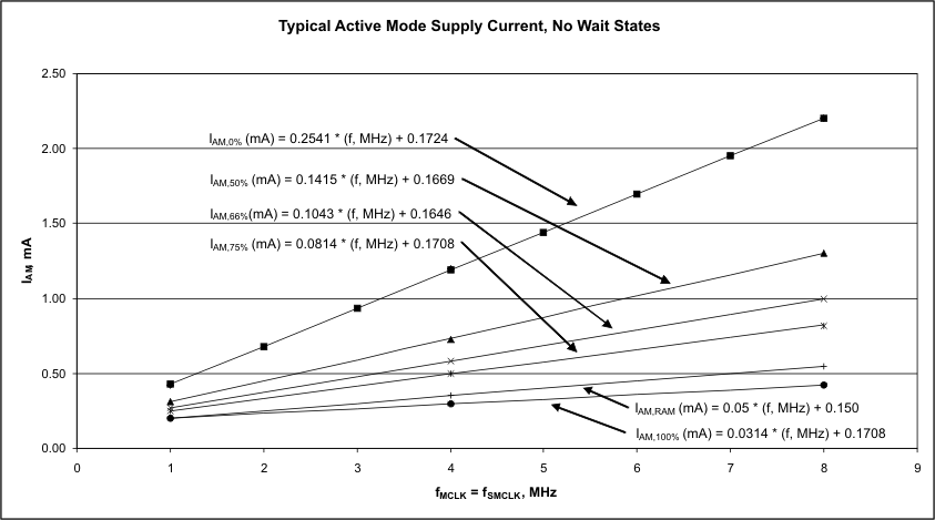 Figure 4-1 Typical Active Mode Supply Currents, No Wait States
4.5 Low-Power Mode Supply Currents (Into VCC) Excluding External Current
over recommended ranges of supply voltage and operating free-air temperature (unless otherwise noted) (1)(2)| PARAMETER | VCC | –55°C | 25°C | 85°C | UNIT | ||||
|---|---|---|---|---|---|---|---|---|---|
| TYP | MAX | TYP | MAX | TYP | MAX | ||||
| ILPM0,1MHz | Low-power mode 0 (3)(12) | 2 V, 3 V |
166 | 175 | 225 | µA | |||
| LPM0,8MHz | Low-power mode 0 (4)(12) | 2 V, 3 V |
170 | 177 | 244 | 225 | 360 | µA | |
| LPM0,24MHz | Low-power mode 0 (5)(12) | 2 V, 3 V |
274 | 285 | 340 | 340 | 455 | µA | |
| ILPM2 | Low-power mode 2 (6)(13) | 2 V, 3 V |
56 | 61 | 80 | 110 | 210 | µA | |
| ILPM3,XT1LF | Low-power mode 3, crystal mode (7)(13) | 2 V, 3 V |
3.4 | 6.4 | 15 | 48 | 150 | µA | |
| ILPM3,VLO | Low-power mode 3, VLO mode (8)(13) | 2 V, 3 V |
3.3 | 6.3 | 15 | 48 | 150 | µA | |
| ILPM4 | Low-power mode 4 (9)(13) | 2 V, 3 V |
2.9 | 5.9 | 15 | 48 | 150 | µA | |
| ILPM3.5 | Low-power mode 3.5 (10) | 2 V, 3 V |
1.3 | 1.5 | 2.2 | 2.8 | 5.0 | µA | |
| ILPM4.5 | Low-power mode 4.5 (11) | 2 V, 3 V |
0.3 | 0.32 | 0.66 | 0.57 | 2.55 | µA | |
(1) All inputs are tied to 0 V or to VCC. Outputs do not source or sink any current.
(2) The currents are characterized with a Micro Crystal CC4V-T1A SMD crystal with a load capacitance of 9 pF. The internal and external load capacitance are chosen to closely match the required 9 pF.
(3) Current for watchdog timer clocked by SMCLK included. ACLK = low-frequency crystal operation (XTS = 0, XT1DRIVEx = 0).
CPUOFF = 1, SCG0 = 0, SCG1 = 0, OSCOFF = 0 (LPM0), ƒACLK = 32768 Hz, ƒMCLK = 0 MHz, ƒSMCLK = 1 MHz. DCORSEL = 0, DCOFSELx = 3 (ƒDCO = 8 MHz)
CPUOFF = 1, SCG0 = 0, SCG1 = 0, OSCOFF = 0 (LPM0), ƒACLK = 32768 Hz, ƒMCLK = 0 MHz, ƒSMCLK = 1 MHz. DCORSEL = 0, DCOFSELx = 3 (ƒDCO = 8 MHz)
(4) Current for watchdog timer clocked by SMCLK included. ACLK = low-frequency crystal operation (XTS = 0, XT1DRIVEx = 0).
CPUOFF = 1, SCG0 = 0, SCG1 = 0, OSCOFF = 0 (LPM0), ƒACLK = 32768 Hz, ƒMCLK = 0 MHz, ƒSMCLK = 8 MHz. DCORSEL = 0, DCOFSELx = 3 (ƒDCO = 8 MHz)
CPUOFF = 1, SCG0 = 0, SCG1 = 0, OSCOFF = 0 (LPM0), ƒACLK = 32768 Hz, ƒMCLK = 0 MHz, ƒSMCLK = 8 MHz. DCORSEL = 0, DCOFSELx = 3 (ƒDCO = 8 MHz)
(5) Current for watchdog timer clocked by SMCLK included. ACLK = low-frequency crystal operation (XTS = 0, XT1DRIVEx = 0).
CPUOFF = 1, SCG0 = 0, SCG1 = 0, OSCOFF = 0 (LPM0), ƒACLK = 32768 Hz, ƒMCLK = 0 MHz, ƒSMCLK = 24 MHz. DCORSEL = 1, DCOFSELx = 3 (ƒDCO = 24 MHz)
CPUOFF = 1, SCG0 = 0, SCG1 = 0, OSCOFF = 0 (LPM0), ƒACLK = 32768 Hz, ƒMCLK = 0 MHz, ƒSMCLK = 24 MHz. DCORSEL = 1, DCOFSELx = 3 (ƒDCO = 24 MHz)
(6) Current for watchdog timer (clocked by ACLK) and RTC (clocked by XT1 LF mode) included. ACLK = low-frequency crystal operation (XTS = 0, XT1DRIVEx = 0).
CPUOFF = 1, SCG0 = 0, SCG1 = 1, OSCOFF = 0 (LPM2), ƒACLK = 32768 Hz, ƒMCLK = 0 MHz, ƒSMCLK = ƒDCO = 0 MHz, DCORSEL = 0, DCOFSELx = 3, DCO bias generator enabled.
CPUOFF = 1, SCG0 = 0, SCG1 = 1, OSCOFF = 0 (LPM2), ƒACLK = 32768 Hz, ƒMCLK = 0 MHz, ƒSMCLK = ƒDCO = 0 MHz, DCORSEL = 0, DCOFSELx = 3, DCO bias generator enabled.
(7) Current for watchdog timer (clocked by ACLK) and RTC (clocked by XT1 LF mode) included. ACLK = low-frequency crystal operation (XTS = 0, XT1DRIVEx = 0).
CPUOFF = 1, SCG0 = 1, SCG1 = 1, OSCOFF = 0 (LPM3), ƒACLK = 32768 Hz, ƒMCLK = ƒSMCLK = ƒDCO = 0 MHz
CPUOFF = 1, SCG0 = 1, SCG1 = 1, OSCOFF = 0 (LPM3), ƒACLK = 32768 Hz, ƒMCLK = ƒSMCLK = ƒDCO = 0 MHz
(8) Current for watchdog timer (clocked by ACLK) included. ACLK = VLO.
CPUOFF = 1, SCG0 = 1, SCG1 = 1, OSCOFF = 0 (LPM3), ƒACLK = ƒVLO, ƒMCLK = ƒSMCLK = ƒDCO = 0 MHz
CPUOFF = 1, SCG0 = 1, SCG1 = 1, OSCOFF = 0 (LPM3), ƒACLK = ƒVLO, ƒMCLK = ƒSMCLK = ƒDCO = 0 MHz
(9) CPUOFF = 1, SCG0 = 1, SCG1 = 1, OSCOFF = 1 (LPM4), ƒDCO = ƒACLK = ƒMCLK = ƒSMCLK = 0 MHz
(10) Internal regulator disabled. No data retention. RTC active clocked by XT1 LF mode.
CPUOFF = 1, SCG0 = 1, SCG1 = 1, OSCOFF = 1, PMMREGOFF = 1 (LPM3.5), ƒDCO = ƒACLK = ƒMCLK = ƒSMCLK = 0 MHz
CPUOFF = 1, SCG0 = 1, SCG1 = 1, OSCOFF = 1, PMMREGOFF = 1 (LPM3.5), ƒDCO = ƒACLK = ƒMCLK = ƒSMCLK = 0 MHz
(11) Internal regulator disabled. No data retention.
CPUOFF = 1, SCG0 = 1, SCG1 = 1, OSCOFF = 1, PMMREGOFF = 1 (LPM4.5), ƒDCO = ƒACLK = ƒMCLK = ƒSMCLK = 0 MHz
CPUOFF = 1, SCG0 = 1, SCG1 = 1, OSCOFF = 1, PMMREGOFF = 1 (LPM4.5), ƒDCO = ƒACLK = ƒMCLK = ƒSMCLK = 0 MHz
(12) Current for brownout, high-side supervisor (SVSH) and low-side supervisor (SVSL) included.
(13) Current for brownout, high-side supervisor (SVSH) included. Low-side supervisor disabled (SVSL).
4.6 Schmitt-Trigger Inputs – General Purpose I/O
(P1.0 to P1.7, P2.0 to P2.7, P3.0 to P3.7, P4.0 to P4.1, PJ.0 to PJ.5, RST/NMI)
over recommended ranges of supply voltage and operating free-air temperature (unless otherwise noted)
| PARAMETER | TEST CONDITIONS | VCC | MIN | TYP | MAX | UNIT | |
|---|---|---|---|---|---|---|---|
| VIT+ | Positive-going input threshold voltage | 2 V | 0.7 | 1.7 | V | ||
| 3 V | 1.45 | 2.12 | |||||
| VIT– | Negative-going input threshold voltage | 2 V | 0.41 | 1.101 | V | ||
| 3 V | 0.72 | 1.68 | |||||
| Vhys | Input voltage hysteresis (VIT+ – VIT–) | 2 V | 0.24 | 0.855 | V | ||
| 3 V | 0.27 | 1.02 | |||||
| RPull | Pullup or pulldown resistor | For pullup: VIN = VSS
For pulldown: VIN = VCC |
19 | 35 | 51 | kΩ | |
| CI | Input capacitance | VIN = VSS or VCC | 5 | pF | |||
4.7 Inputs – Ports P1 and P2 (1)
(P1.0 to P1.7, P2.0 to P2.7)
over recommended ranges of supply voltage and operating free-air temperature (unless otherwise noted)
| PARAMETER | TEST CONDITIONS | VCC | MIN | MAX | UNIT | |
|---|---|---|---|---|---|---|
| t(int) | External interrupt timing (2) | External trigger pulse duration to set interrupt flag | 2 V, 3 V | 20 | ns | |
(1) Some devices may contain additional ports with interrupts. See the block diagram and terminal function descriptions.
(2) An external signal sets the interrupt flag every time the minimum interrupt pulse duration t(int) is met. It may be set by trigger signals shorter than t(int).
4.8 Leakage Current – General Purpose I/O
(P1.0 to P1.7, P2.0 to P2.7, P3.0 to P3.7, P4.0 to P4.1, PJ.0 to PJ.5, RST/NMI)
over recommended ranges of supply voltage and operating free-air temperature (unless otherwise noted)
| PARAMETER | TEST CONDITIONS | VCC | MIN | MAX | UNIT | |
|---|---|---|---|---|---|---|
| Ilkg(Px.x) | High-impedance leakage current | (1)(2) | 2 V, 3 V | –65 | 65 | nA |
(1) The leakage current is measured with VSS or VCC applied to the corresponding pin(s), unless otherwise noted.
(2) The leakage of the digital port pins is measured individually. The port pin is selected for input and the pullup/pulldown resistor is disabled.
4.9 Outputs – General Purpose I/O
(P1.0 to P1.7, P2.0 to P2.7, P3.0 to P3.7, P4.0 to P4.1, PJ.0 to PJ.5)
over recommended ranges of supply voltage and operating free-air temperature (unless otherwise noted)
| PARAMETER | TEST CONDITIONS | VCC | MIN | MAX | UNIT | |
|---|---|---|---|---|---|---|
| VOH | High-level output voltage | I(OHmax) = –1 mA (1) | 2 V | VCC – 0.25 | VCC | V |
| I(OHmax) = –3 mA (2) | VCC – 0.60 | VCC | ||||
| I(OHmax) = –2 mA (1) | 3 V | VCC – 0.25 | VCC | |||
| I(OHmax) = –6 mA (2) | VCC – 0.60 | VCC | ||||
| VOL | Low-level output voltage | I(OLmax) = 1 mA (1) | 2 V | VSS | VSS + 0.25 | V |
| I(OLmax) = 3 mA (2) | VSS | VSS + 0.60 | ||||
| I(OLmax) = 2 mA (1) | 3 V | VSS | VSS + 0.25 | |||
| I(OLmax) = 6 mA (2) | VSS | VSS + 0.60 | ||||
(1) The maximum total current, I(OHmax) and I(OLmax), for all outputs combined, should not exceed ±48 mA to hold the maximum voltage drop specified.
(2) The maximum total current, I(OHmax) and I(OLmax), for all outputs combined, should not exceed ±100 mA to hold the maximum voltage drop specified.
4.10 Output Frequency – General Purpose I/O
(P1.0 to P1.7, P2.0 to P2.7, P3.0 to P3.7, P4.0 to P4.1, PJ.0 to PJ.5)
over recommended ranges of supply voltage and operating free-air temperature (unless otherwise noted)
| PARAMETER | TEST CONDITIONS | VCC | MIN | MAX | UNIT | |
|---|---|---|---|---|---|---|
| ƒPx.y | Port output frequency (with load) | Px.y (1)(2) | 2 V | 16 | MHz | |
| 3 V | 24 | |||||
| ƒPort_CLK | Clock output frequency | ACLK, SMCLK, or MCLK at configured output port, CL = 20 pF, no DC loading (2) |
2 V | 16 | MHz | |
| 3 V | 24 | |||||
(1) A resistive divider with 2 × 1.6 kΩ between VCC and VSS is used as load. The output is connected to the center tap of the divider. CL = 20 pF is connected from the output to VSS.
(2) The output voltage reaches at least 10% and 90% VCC at the specified toggle frequency.
4.11 Typical Characteristics – Outputs
over recommended ranges of supply voltage and operating free-air temperature (unless otherwise noted)
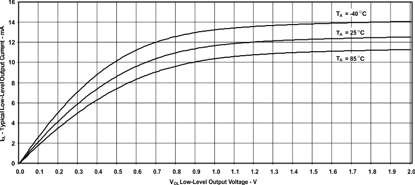
| VCC = 2.0 V | Measured at Px.y |
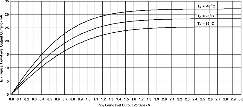
| VCC = 3.0 V | Measured at Px.y |
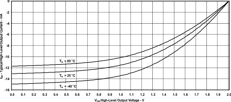
| VCC = 2.0 V | Measured at Px.y |
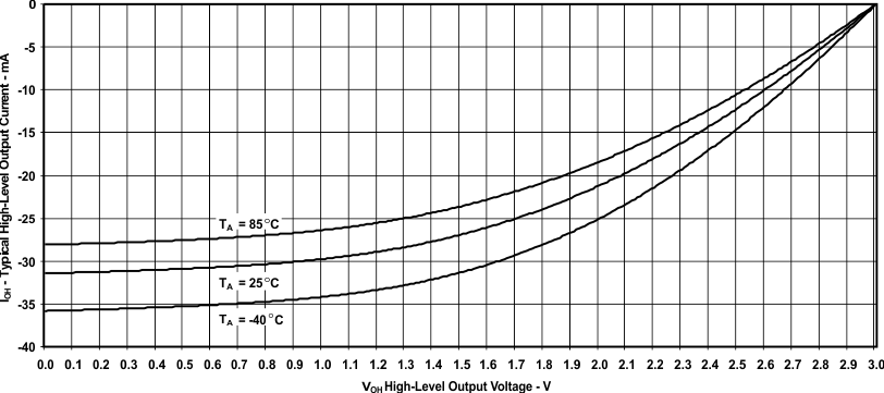
| VCC = 3.0 V | Measured at Px.y |
4.12 Crystal Oscillator, XT1, Low-Frequency (LF) Mode(5)
over recommended ranges of supply voltage and operating free-air temperature (unless otherwise noted)(10)| PARAMETER | TEST CONDITIONS | VCC | MIN | TYP | MAX | UNIT | |
|---|---|---|---|---|---|---|---|
| ΔIVCC.LF | Additional current consumption XT1 LF mode from lowest drive setting | ƒOSC = 32768 Hz, XTS = 0, XT1BYPASS = 0, XT1DRIVE = {1}, CL,eff = 9 pF, TA = 25°C, |
3 V | 60 | nA | ||
| ƒOSC = 32768 Hz, XTS = 0, XT1BYPASS = 0, XT1DRIVE = {2}, TA = 25°C, CL,eff = 9 pF |
3 V | 90 | |||||
| ƒOSC = 32768 Hz, XTS = 0, XT1BYPASS = 0, XT1DRIVE = {3}, TA = 25°C, CL,eff = 12 pF |
3 V | 140 | |||||
| ƒXT1,LF0 | XT1 oscillator crystal frequency, LF mode | XTS = 0, XT1BYPASS = 0 | 32768 | Hz | |||
| ƒXT1,LF,SW | XT1 oscillator logic-level square-wave input frequency, LF mode | XTS = 0, XT1BYPASS = 1 (6)(7) | 10 | 32.768 | 50 | kHz | |
| OALF | Oscillation allowance for LF crystals (8) | XTS = 0, XT1BYPASS = 0, XT1DRIVE = {0}, ƒXT1,LF = 32768 Hz, CL,eff = 6 pF |
210 | kΩ | |||
| XTS = 0, XT1BYPASS = 0, XT1DRIVE = {3}, ƒXT1,LF = 32768 Hz, CL,eff = 12 pF |
300 | ||||||
| Duty cycle, LF mode | XTS = 0, Measured at ACLK, ƒXT1,LF = 32768 Hz |
30 | 70 | % | |||
| ƒFault,LF | Oscillator fault frequency, LF mode (4) | XTS = 0 (3) | 10 | 10000 | Hz | ||
| tSTART,LF | Startup time, LF mode (9) | ƒOSC = 32768 Hz, XTS = 0, XT1BYPASS = 0, XT1DRIVE = {0}, TA = 25°C, CL,eff = 6 pF |
3 V | 1000 | ms | ||
| ƒOSC = 32768 Hz, XTS = 0, XT1BYPASS = 0, XT1DRIVE = {3}, TA = 25°C, CL,eff = 12 pF |
1000 | ||||||
| CL,eff | Integrated effective load capacitance, LF mode (1)(2) | XTS = 0 | 1 | pF | |||
(1) Requires external capacitors at both terminals.
(2) Values are specified by crystal manufacturers. Include parasitic bond and package capacitance (approximately 2 pF per pin). Recommended values supported are 6 pF, 9 pF, and 12 pF. Maximum shunt capacitance of 1.6 pF.
(3) Measured with logic-level input frequency but also applies to operation with crystals.
(4) Frequencies below the MIN specification set the fault flag. Frequencies above the MAX specification do not set the fault flag. Frequencies in between might set the flag.
(5) To improve EMI on the XT1 oscillator, the following guidelines should be observed.
- Keep the trace between the device and the crystal as short as possible.
- Design a good ground plane around the oscillator pins.
- Prevent crosstalk from other clock or data lines into oscillator pins XIN and XOUT.
- Avoid running PCB traces underneath or adjacent to the XIN and XOUT pins.
- Use assembly materials and processes that avoid any parasitic load on the oscillator XIN and XOUT pins.
- If conformal coating is used, ensure that it does not induce capacitive or resistive leakage between the oscillator pins.
(6) When XT1BYPASS is set, XT1 circuits are automatically powered down. Input signal is a digital square wave with parametrics defined in the Schmitt-trigger Inputs section of this data sheet.
(7) Maximum frequency of operation of the entire device cannot be exceeded.
(8) Oscillation allowance is based on a safety factor of 5 for recommended crystals. The oscillation allowance is a function of the XT1DRIVE settings and the effective load. In general, comparable oscillator allowance can be achieved based on the following guidelines, but should be evaluated based on the actual crystal selected for the application:
- For XT1DRIVE = {0}, CL,eff ≤ 6 pF.
- For XT1DRIVE = {1}, 6 pF ≤ CL,eff ≤ 9 pF.
- For XT1DRIVE = {2}, 6 pF ≤ CL,eff ≤ 10 pF.
- For XT1DRIVE = {3}, 6 pF ≤ CL,eff ≤ 12 pF.
(9) Includes startup counter of 4096 clock cycles.
(10) –40°C to 85°C
4.13 Crystal Oscillator, XT1, High-Frequency (HF) Mode(5)
over recommended ranges of supply voltage and operating free-air temperature (unless otherwise noted)(10)| PARAMETER | TEST CONDITIONS | VCC | MIN | TYP | MAX | UNIT | |
|---|---|---|---|---|---|---|---|
| IVCC,HF | XT1 oscillator crystal current HF mode | ƒOSC = 4 MHz, XTS = 1, XOSCOFF = 0, XT1BYPASS = 0, XT1DRIVE = {0}, TA = 25°C, CL,eff = 16 pF |
3 V | 175 | µA | ||
| ƒOSC = 8 MHz, XTS = 1, XOSCOFF = 0, XT1BYPASS = 0, XT1DRIVE = {1}, TA = 25°C, CL,eff = 16 pF |
300 | ||||||
| ƒOSC = 16 MHz, XTS = 1, XOSCOFF = 0, XT1BYPASS = 0, XT1DRIVE = {2}, TA = 25°C, CL,eff = 16 pF |
350 | ||||||
| ƒOSC = 24 MHz, XTS = 1, XOSCOFF = 0, XT1BYPASS = 0, XT1DRIVE = {3}, TA = 25°C, CL,eff = 16 pF |
550 | ||||||
| ƒXT1,HF0 | XT1 oscillator crystal frequency, HF mode 0 | XTS = 1, XT1BYPASS = 0, XT1DRIVE = {0} (7) |
4 | 6 | MHz | ||
| ƒXT1,HF1 | XT1 oscillator crystal frequency, HF mode 1 | XTS = 1, XT1BYPASS = 0, XT1DRIVE = {1} (7) |
6 | 10 | MHz | ||
| ƒXT1,HF2 | XT1 oscillator crystal frequency, HF mode 2 | XTS = 1, XT1BYPASS = 0, XT1DRIVE = {2} (7) |
10 | 16 | MHz | ||
| ƒXT1,HF3 | XT1 oscillator crystal frequency, HF mode 3 | XTS = 1, XT1BYPASS = 0, XT1DRIVE = {3} (7) |
16 | 24 | MHz | ||
| ƒXT1,HF,SW | XT1 oscillator logic-level square-wave input frequency, HF mode | XTS = 1, XT1BYPASS = 1 (6)(7) |
1 | 24 | MHz | ||
| OAHF | Oscillation allowance for HF crystals (8) | XTS = 1, XT1BYPASS = 0, XT1DRIVE = {0}, ƒXT1,HF = 4 MHz, CL,eff = 16 pF |
450 | Ω | |||
| XTS = 1, XT1BYPASS = 0, XT1DRIVE = {1}, ƒXT1,HF = 8 MHz, CL,eff = 16 pF |
320 | ||||||
| XTS = 1, XT1BYPASS = 0, XT1DRIVE = {2}, ƒXT1,HF = 16 MHz, CL,eff = 16 pF |
200 | ||||||
| XTS = 1, XT1BYPASS = 0, XT1DRIVE = {3}, ƒXT1,HF = 24 MHz, CL,eff = 16 pF |
200 | ||||||
| tSTART,HF | Startup time, HF mode (9) | ƒOSC = 4 MHz, XTS = 1, XT1BYPASS = 0, XT1DRIVE = {0}, TA = 25°C, CL,eff = 16 pF |
3 V | 8 | ms | ||
| ƒOSC = 24 MHz, XTS = 1, XT1BYPASS = 0, XT1DRIVE = {3}, TA = 25°C, CL,eff = 16 pF |
2 | ||||||
| CL,eff | Integrated effective load capacitance (1)(2) | XTS = 1 | 1 | pF | |||
| Duty cycle, HF mode | XTS = 1, Measured at ACLK, ƒXT1,HF2 = 24 MHz |
40 | 50 | 60 | % | ||
| ƒFault,HF | Oscillator fault frequency, HF mode (4) | XTS = 1 (3) | 145 | 900 | kHz | ||
(1) Includes parasitic bond and package capacitance (approximately 2 pF per pin). Because the PCB adds additional capacitance, it is recommended to verify the correct load by measuring the ACLK frequency. For a correct setup, the effective load capacitance should always match the specification of the used crystal.
(2) Requires external capacitors at both terminals. Values are specified by crystal manufacturers. Recommended values supported are 14 pF, 16 pF, and 18 pF. Maximum shunt capacitance of 7 pF.
(3) Measured with logic-level input frequency but also applies to operation with crystals.
(4) Frequencies below the MIN specification set the fault flag. Frequencies above the MAX specification do not set the fault flag. Frequencies in between might set the flag.
(5) To improve EMI on the XT1 oscillator the following guidelines should be observed.
- Keep the traces between the device and the crystal as short as possible.
- Design a good ground plane around the oscillator pins.
- Prevent crosstalk from other clock or data lines into oscillator pins XIN and XOUT.
- Avoid running PCB traces underneath or adjacent to the XIN and XOUT pins.
- Use assembly materials and processes that avoid any parasitic load on the oscillator XIN and XOUT pins.
- If conformal coating is used, ensure that it does not induce capacitive or resistive leakage between the oscillator pins.
(6) When XT1BYPASS is set, XT1 circuits are automatically powered down. Input signal is a digital square wave with parametrics defined in the Schmitt-trigger Inputs section of this data sheet.
(7) Maximum frequency of operation of the entire device cannot be exceeded.
(8) Oscillation allowance is based on a safety factor of 5 for recommended crystals.
(9) Includes startup counter of 4096 clock cycles.
(10) –40°C to 85°C
4.14 Internal Very-Low-Power Low-Frequency Oscillator (VLO)
over recommended ranges of supply voltage and operating free-air temperature (unless otherwise noted)| PARAMETER | TEST CONDITIONS | VCC | MIN | TYP | MAX | UNIT | |
|---|---|---|---|---|---|---|---|
| ƒVLO | VLO frequency | Measured at ACLK | 2 V to 3.6 V | 4.3 | 8.3 | 13.3 | kHz |
| dƒVLO/dT | VLO frequency temperature drift | Measured at ACLK (1) | 2 V to 3.6 V | 0.5 | %/°C | ||
| dƒVLO/dVCC | VLO frequency supply voltage drift | Measured at ACLK (2) | 2 V to 3.6 V | 4 | %/V | ||
| ƒVLO,DC | Duty cycle | Measured at ACLK | 2 V to 3.6 V | 35% | 50% | 65% | |
(1) Calculated using the box method: (MAX(–55 to 85°C) – MIN(–55 to 85°C)) / MIN(–55 to 85°C) / (85°C – (–55°C))
(2) Calculated using the box method: (MAX(2.0 to 3.6 V) – MIN(2.0 to 3.6 V)) / MIN(2.0 to 3.6 V) / (3.6 V – 2 V)
4.15 DCO Frequencies
over recommended ranges of supply voltage and operating free-air temperature (unless otherwise noted)| PARAMETER | TEST CONDITIONS | VCC
TA |
MIN | TYP | MAX | UNIT | |
|---|---|---|---|---|---|---|---|
| ƒDCO,LO | DCO frequency low, trimmed | Measured at ACLK, DCORSEL = 0 |
2 V to 3.6 V –55°C to 85°C |
5.37 | ±5% | MHz | |
| Measured at ACLK, DCORSEL = 1 |
2 V to 3.6 V –55°C to 85°C |
16.2 | ±5% | MHz | |||
| ƒDCO,MID | DCO frequency mid, trimmed | Measured at ACLK, DCORSEL = 0 |
2 V to 3.6 V –55°C to 85°C |
6.67 | ±5% | MHz | |
| Measured at ACLK, DCORSEL = 1 |
2 V to 3.6 V –55°C to 85°C |
20 | ±5% | MHz | |||
| ƒDCO,HI | DCO frequency high, trimmed | Measured at ACLK, DCORSEL = 0 |
2 V to 3.6 V –55°C to 85°C |
8 | ±5% | MHz | |
| Measured at ACLK, DCORSEL = 1 |
2 V to 3.6 V –55°C to 85°C |
23.8 | ±5% | MHz | |||
| ƒDCO,DC | Duty cycle | Measured at ACLK, divide by 1, No external divide, all DCO settings |
2 V to 3.6 V –55°C to 85°C |
35% | 50% | 65% | |
4.16 MODOSC
over operating free-air temperature range (unless otherwise noted)| PARAMETER | TEST CONDITIONS | VCC | MIN | TYP | MAX | UNIT | |
|---|---|---|---|---|---|---|---|
| IMODOSC | Current consumption | Enabled | 2 V to 3.6 V | 44 | µA | ||
| ƒMODOSC | MODOSC frequency | 2 V to 3.6 V | 4.2 | 5.0 | 5.7 | MHz | |
| ƒMODOSC,DC | Duty cycle | Measured at ACLK, divide by 1 | 2 V to 3.6 V | 35% | 50% | 65% | |
4.17 PMM, Core Voltage
over recommended ranges of supply voltage and operating free-air temperature (unless otherwise noted)| PARAMETER | TEST CONDITIONS | MIN | TYP | MAX | UNIT | |
|---|---|---|---|---|---|---|
| VCORE(AM) | Core voltage, active mode | 2 V ≤ DVCC ≤ 3.6 V | 1.5 | V | ||
| VCORE(LPM) | Core voltage, low-current mode | 2 V ≤ DVCC ≤ 3.6 V | 1.5 | V | ||
4.18 PMM, SVS, BOR
over recommended ranges of supply voltage and operating free-air temperature (unless otherwise noted)| PARAMETER | TEST CONDITIONS | MIN | TYP | MAX | UNIT | |
|---|---|---|---|---|---|---|
| ISVSH,AM | SVSH current consumption, active mode | VCC = 3.6 V | 5 | µA | ||
| ISVSH,LPM | SVSH current consumption, low power modes | VCC = 3.6 V | 0.8 | µA | ||
| VSVSH- | SVSH on voltage level, falling supply voltage | 1.81 | 1.88 | 1.95 | V | |
| VSVSH+ | SVSH off voltage level, rising supply voltage | 1.85 | 1.93 | 2 | V | |
| tPD,SVSH, AM | SVSH propagation delay, active mode | dVCC/dt = 10 mV/µs | 10 | µs | ||
| tPD,SVSH, LPM | SVSH propagation delay, low power modes | dVCC/dt = 1 mV/µs | 30 | µs | ||
| ISVSL | SVSL current consumption | 0.3 | µA | |||
| VSVSL– | SVSL on voltage level | 1.42 | V | |||
| VSVSL+ | SVSL off voltage level | 1.47 | V | |||
4.19 Wake-Up from Low Power Modes
over recommended ranges of supply voltage and operating free-air temperature (unless otherwise noted)| PARAMETER | TEST CONDITIONS | VCC
TA |
MIN | TYP | MAX | UNIT | |
|---|---|---|---|---|---|---|---|
| tWAKE-UP LPM0 | Wake-up time from LPM0 to active mode (1) | 2 V, 3 V –55°C to 85°C |
0.58 | 1.1 | µs | ||
| tWAKE-UP LPM12 | Wake-up time from LPM1, LPM2 to active mode (1) | 2 V, 3 V –55°C to 85°C |
12 | 25 | µs | ||
| tWAKE-UP LPM34 | Wake-up time from LPM3 or LPM4 to active mode (1) | 2 V, 3 V –55°C to 85°C |
78 | 165 | µs | ||
| tWAKE-UP LPMx.5 | Wake-up time from LPM3.5 or LPM4.5 to active mode (1) | 2 V, 3 V 0°C to 85°C |
310 | 575 | µs | ||
| 2 V, 3 V –55°C to 85°C |
310 | 1100 | µs | ||||
| tWAKE-UP RESET | Wake-up time from RST to active mode (2) | VCC stable |
2 V, 3 V –55°C to 85°C |
230 | µs | ||
| tWAKE-UP BOR | Wake-up time from BOR or power-up to active mode | dVCC/dt = 2400 V/s | 2 V, 3 V –55°C to 85°C |
1.6 | ms | ||
| tRESET | Pulse duration required at RST/NMI terminal to accept a reset event(3) | 2 V, 3 V –55°C to 85°C |
4 | ns | |||
(1) The wake-up time is measured from the edge of an external wake-up signal (for example, port interrupt or wake-up event) until the first instruction of the user program is executed.
(2) The wake-up time is measured from the rising edge of the RST signal until the first instruction of the user program is executed.
(3) Meeting or exceeding this time makes sures a reset event occurs. Pulses shorter than this minimum time may or may not cause a reset event to occur.
4.20 Timer_A
over recommended ranges of supply voltage and operating free-air temperature (unless otherwise noted)| PARAMETER | TEST CONDITIONS | VCC | MIN | TYP | MAX | UNIT | |
|---|---|---|---|---|---|---|---|
| ƒTA | Timer_A input clock frequency | Internal: SMCLK, ACLK External: TACLK Duty cycle = 50% ± 10% |
2 V, 3 V | 24 | MHz | ||
| tTA,cap | Timer_A capture timing | All capture inputs, Minimum pulse duration required for capture | 2 V, 3 V | 20 | ns | ||
4.21 Timer_B
over recommended ranges of supply voltage and operating free-air temperature (unless otherwise noted)| PARAMETER | TEST CONDITIONS | VCC | MIN | TYP | MAX | UNIT | |
|---|---|---|---|---|---|---|---|
| ƒTB | Timer_B input clock frequency | Internal: SMCLK, ACLK External: TBCLK Duty cycle = 50% ± 10% |
2 V, 3 V | 24 | MHz | ||
| tTB,cap | Timer_B capture timing | All capture inputs, Minimum pulse duration required for capture | 2 V, 3 V | 20 | ns | ||
4.22 eUSCI (UART Mode) Recommended Operating Conditions
| PARAMETER | CONDITIONS | VCC | MIN | TYP | MAX | UNIT | |
|---|---|---|---|---|---|---|---|
| ƒeUSCI | eUSCI input clock frequency | Internal: SMCLK, ACLK External: UCLK Duty cycle = 50% ± 10% |
ƒSYSTEM | MHz | |||
| ƒBITCLK | BITCLK clock frequency (equals baud rate in MBaud) |
5 | MHz | ||||
4.23 eUSCI (UART Mode)
over recommended ranges of supply voltage and operating free-air temperature (unless otherwise noted)| PARAMETER | TEST CONDITIONS | VCC | MIN | TYP | MAX | UNIT | |
|---|---|---|---|---|---|---|---|
| tt | UART receive deglitch time(1) | UCGLITx = 0 | 2 V, 3 V | 5 | 15 | 20 | ns |
| UCGLITx = 1 | 20 | 45 | 60 | ||||
| UCGLITx = 2 | 35 | 80 | 120 | ||||
| UCGLITx = 3 | 50 | 110 | 180 | ||||
(1) Pulses on the UART receive input (UCxRX) shorter than the UART receive deglitch time are suppressed. To ensure that pulses are correctly recognized, their duration should exceed the maximum specification of the deglitch time.
4.24 eUSCI (SPI Master Mode) Recommended Operating Conditions
| PARAMETER | CONDITIONS | VCC | MIN | TYP | MAX | UNIT | |
|---|---|---|---|---|---|---|---|
| ƒeUSCI | eUSCI input clock frequency | Internal: SMCLK, ACLK Duty cycle = 50% ± 10% |
ƒSYSTEM | MHz | |||
4.25 eUSCI (SPI Master Mode)
over recommended ranges of supply voltage and operating free-air temperature (unless otherwise noted) (1)| PARAMETER | TEST CONDITIONS | VCC | MIN | TYP | MAX | UNIT | |
|---|---|---|---|---|---|---|---|
| tSTE,LEAD | STE lead time, STE active to clock | UCSTEM = 0, UCMODEx = 01 or 10 |
2 V, 3 V | 1 | UCxCLK cycles | ||
| UCSTEM = 1, UCMODEx = 01 or 10 |
2 V, 3 V | 1 | |||||
| tSTE,LAG | STE lag time, Last clock to STE inactive | UCSTEM = 0, UCMODEx = 01 or 10 |
2 V, 3 V | 1 | UCxCLK cycles | ||
| UCSTEM = 1, UCMODEx = 01 or 10 |
2 V, 3 V | 1 | |||||
| tSTE,ACC | STE access time, STE active to SIMO data out | UCSTEM = 0, UCMODEx = 01 or 10 |
2 V, 3 V | 55 | ns | ||
| UCSTEM = 1, UCMODEx = 01 or 10 |
2 V, 3 V | 35 | |||||
| tSTE,DIS | STE disable time, STE inactive to SIMO high impedance | UCSTEM = 0, UCMODEx = 01 or 10 |
2 V, 3 V | 40 | ns | ||
| UCSTEM = 1, UCMODEx = 01 or 10 |
2 V, 3 V | 30 | |||||
| tSU,MI | SOMI input data setup time | 2 V | 35 | ns | |||
| 3 V | 35 | ||||||
| tHD,MI | SOMI input data hold time | 2 V | 0 | ns | |||
| 3 V | 0 | ||||||
| tVALID,MO | SIMO output data valid time (2) | UCLK edge to SIMO valid, CL = 20 pF |
2 V | 30 | ns | ||
| 3 V | 30 | ||||||
| tHD,MO | SIMO output data hold time (3) | CL = 20 pF | 2 V | 0 | ns | ||
| 3 V | 0 | ||||||
(1) ƒUCxCLK = 1/2tLO/HI with tLO/HI = max(tVALID,MO(eUSCI) + tSU,SI(Slave), tSU,MI(eUSCI) + tVALID,SO(Slave)).
For the slave's parameters tSU,SI(Slave) and tVALID,SO(Slave) see the SPI parameters of the attached slave.
For the slave's parameters tSU,SI(Slave) and tVALID,SO(Slave) see the SPI parameters of the attached slave.
(2) Specifies the time to drive the next valid data to the SIMO output after the output changing UCLK clock edge. See the timing diagrams in Figure 4-6 and Figure 4-7.
(3) Specifies how long data on the SIMO output is valid after the output changing UCLK clock edge. Negative values indicate that the data on the SIMO output can become invalid before the output changing clock edge observed on UCLK. See the timing diagrams in Figure 4-6 and Figure 4-7.
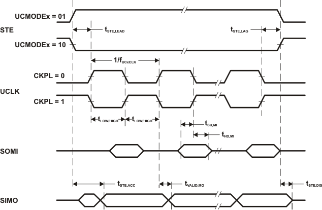 Figure 4-6 SPI Master Mode, CKPH = 0
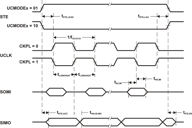 Figure 4-7 SPI Master Mode, CKPH = 1
4.26 eUSCI (SPI Slave Mode)
over recommended ranges of supply voltage and operating free-air temperature (unless otherwise noted) (1)| PARAMETER | TEST CONDITIONS | VCC | MIN | TYP | MAX | UNIT | |
|---|---|---|---|---|---|---|---|
| tSTE,LEAD | STE lead time, STE active to clock | 2 V | 7 | ns | |||
| 3 V | 7 | ||||||
| tSTE,LAG | STE lag time, Last clock to STE inactive | 2 V | 0 | ns | |||
| 3 V | 0 | ||||||
| tSTE,ACC | STE access time, STE active to SOMI data out | 2 V | 65 | ns | |||
| 3 V | 40 | ||||||
| tSTE,DIS | STE disable time, STE inactive to SOMI high impedance | 2 V | 40 | ns | |||
| 3 V | 35 | ||||||
| tSU,SI | SIMO input data setup time | 2 V | 2 | ns | |||
| 3 V | 2 | ||||||
| tHD,SI | SIMO input data hold time | 2 V | 5 | ns | |||
| 3 V | 5 | ||||||
| tVALID,SO | SOMI output data valid time (2) | UCLK edge to SOMI valid, CL = 20 pF |
2 V | 30 | ns | ||
| 3 V | 30 | ||||||
| tHD,SO | SOMI output data hold time (3) | CL = 20 pF | 2 V | 4 | ns | ||
| 3 V | 4 | ||||||
(1) ƒUCxCLK = 1/2tLO/HI with tLO/HI ≥ max(tVALID,MO(Master) + tSU,SI(eUSCI), tSU,MI(Master) + tVALID,SO(eUSCI)).
For the master's parameters tSU,MI(Master) and tVALID,MO(Master) see the SPI parameters of the attached slave.
For the master's parameters tSU,MI(Master) and tVALID,MO(Master) see the SPI parameters of the attached slave.
(2) Specifies the time to drive the next valid data to the SOMI output after the output changing UCLK clock edge. See the timing diagrams in Figure 4-8 and Figure 4-9.
(3) Specifies how long data on the SOMI output is valid after the output changing UCLK clock edge. See the timing diagrams in Figure 4-8 and Figure 4-9.
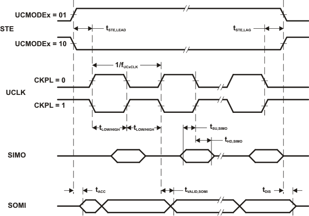 Figure 4-8 SPI Slave Mode, CKPH = 0
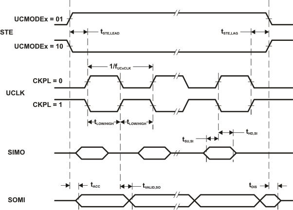 Figure 4-9 SPI Slave Mode, CKPH = 1
4.27 eUSCI (I2C Mode)
over recommended ranges of supply voltage and operating free-air temperature (unless otherwise noted) (see Figure 4-10)| PARAMETER | TEST CONDITIONS | VCC | MIN | TYP | MAX | UNIT | |
|---|---|---|---|---|---|---|---|
| ƒeUSCI | eUSCI input clock frequency | Internal: SMCLK, ACLK External: UCLK Duty cycle = 50% ±10% |
ƒSYSTEM | MHz | |||
| ƒSCL | SCL clock frequency | 2 V, 3 V | 0 | 400 | kHz | ||
| tHD,STA | Hold time (repeated) START | ƒSCL = 100 kHz | 2 V, 3 V | 4.0 | µs | ||
| ƒSCL > 100 kHz | 0.6 | ||||||
| tSU,STA | Setup time for a repeated START | ƒSCL = 100 kHz | 2 V, 3 V | 4.7 | µs | ||
| ƒSCL > 100 kHz | 0.6 | ||||||
| tHD,DAT | Data hold time | 2 V, 3 V | 0 | ns | |||
| tSU,DAT | Data setup time | 2 V, 3 V | 250 | ns | |||
| tSU,STO | Setup time for STOP | ƒSCL = 100 kHz | 2 V, 3 V | 4.0 | µs | ||
| ƒSCL > 100 kHz | 0.6 | ||||||
| tSP | Pulse duration of spikes suppressed by input filter | UCGLITx = 0 | 2 V, 3 V | 50 | 600 | ns | |
| UCGLITx = 1 | 25 | 300 | ns | ||||
| UCGLITx = 2 | 12.5 | 150 | ns | ||||
| UCGLITx = 3 | 6.25 | 75 | ns | ||||
| tTIMEOUT | Clock low timeout | UCCLTOx = 1 | 2 V, 3 V | 27 | ms | ||
| UCCLTOx = 2 | 30 | ms | |||||
| UCCLTOx = 3 | 33 | ms | |||||
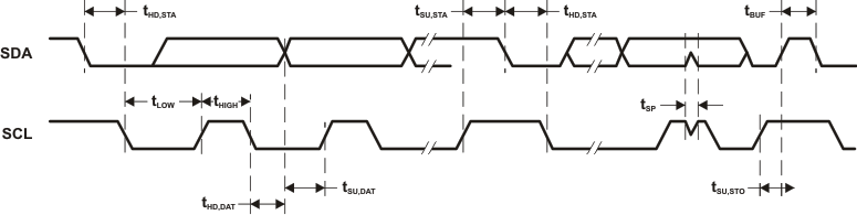 Figure 4-10 I2C Mode Timing
4.28 10-Bit ADC, Power Supply and Input Range Conditions
over operating free-air temperature range (unless otherwise noted)| PARAMETER | TEST CONDITIONS | VCC | MIN | TYP | MAX | UNIT | |
|---|---|---|---|---|---|---|---|
| AVCC | Analog supply voltage | AVCC and DVCC are connected together, AVSS and DVSS are connected together, V(AVSS) = V(DVSS) = 0 V |
2.0 | 3.6 | V | ||
| V(Ax) | Analog input voltage range | All ADC10 pins | 0 | AVCC | V | ||
| IADC10_A | Operating supply current into AVCC terminal, reference current not included | ƒADC10CLK = 5 MHz, ADC10ON = 1, REFON = 0, SHT0 = 0, SHT1 = 0, ADC10DIV = 0 |
2 V | 90 | 150 | µA | |
| 3 V | 100 | 170 | |||||
| CI | Input capacitance | Only one terminal Ax can be selected at one time from the pad to the ADC10_A capacitor array including wiring and pad | 2.2 V | 6 | pF | ||
| RI | Input MUX ON resistance | AVCC ≥ 2 V, 0 V ≤ VAx ≤ AVCC | 36 | kΩ | |||
4.29 10-Bit ADC, Timing Parameters
over operating free-air temperature range (unless otherwise noted)| PARAMETER | TEST CONDITIONS | VCC | MIN | TYP | MAX | UNIT | |
|---|---|---|---|---|---|---|---|
| ƒADC10CLK | For specified performance of ADC10 linearity parameters | 2 V to 3.6 V | 0.45 | 5 | 5.5 | MHz | |
| ƒADC10OSC | Internal ADC10 oscillator (MODOSC) | ADC10DIV = 0, ƒADC10CLK = ƒADC10OSC | 2 V to 3.6 V | 4.2 | 4.5 | 5.7 | MHz |
| tCONVERT | Conversion time | REFON = 0, Internal oscillator, 12 ADC10CLK cycles, 10-bit mode, ƒADC10OSC = 4.5 MHz to 5.5 MHz |
2 V to 3.6 V | 2.18 | 2.67 | µs | |
| External ƒADC10CLK from ACLK, MCLK, or SMCLK, ADC10SSEL ≠ 0 | 2 V to 3.6 V | (1) | |||||
| tADC10ON | Turn on settling time of the ADC | The error in a conversion started after tADC10ON is less than ±0.5 LSB, Reference and input signal already settled |
100 | ns | |||
| tSample | Sampling time | RS = 1000 Ω, RI = 36000 Ω, CI = 3.5 pF, Approximately eight Tau (τ) are required to get an error of less than ±0.5 LSB |
2 V | 1.5 | µs | ||
| 3 V | 2.0 | ||||||
(1) 12 × ADC10DIV × 1/ƒADC10CLK
4.30 10-Bit ADC, Linearity Parameters
over operating free-air temperature range (unless otherwise noted)| PARAMETER | TEST CONDITIONS | VCC | MIN | TYP | MAX | UNIT | |
|---|---|---|---|---|---|---|---|
| EI | Integral linearity error | 1.4 V ≤ (VeREF+ – VREF–/VeREF–)min ≤ 1.6 V | 3.6 V | –1.4 | 1.4 | LSB | |
| 1.6 V < (VeREF+ – VREF–/VeREF–)min ≤ VAVCC | –1.3 | 1.3 | |||||
| ED | Differential linearity error | (VeREF+ – VREF–/VeREF–)min ≤ (VeREF+ – VREF–/VeREF–) | 3.6 V | –1.2 | 1.2 | LSB | |
| EO | Offset error | (VeREF+ – VREF–/VeREF–)min ≤ (VeREF+ – VREF–/VeREF–) | 3.6 V | ±2.5 | mV | ||
| EG | Gain error, external reference | (VeREF+ – VREF–/VeREF–)min ≤ (VeREF+ – VREF–/VeREF–) | 3.6 V | –1.4 | 1.4 | LSB | |
| Gain error, internal reference (1) | ±4 | ||||||
| ET | Total unadjusted error, external reference | (VeREF+ – VREF–/VeREF–)min ≤ (VeREF+ – VREF–/VeREF–) | 3.6 V | ±2.3 | LSB | ||
| Total unadjusted error, internal reference (1) | ±4 | ||||||
(1) Error is dominated by the internal reference.
4.31 REF, External Reference
over recommended ranges of supply voltage and operating free-air temperature (unless otherwise noted) (1)| PARAMETER | TEST CONDITIONS | VCC | MIN | TYP | MAX | UNIT | |
|---|---|---|---|---|---|---|---|
| VeREF+ | Positive external reference voltage input | VeREF+ > VeREF–(2) | 1.4 | AVCC | V | ||
| VeREF– | Negative external reference voltage input | VeREF+ > VeREF–(3) | 0 | 1.2 | V | ||
| (VeREF+ – VREF–/VeREF–) |
Differential external reference voltage input | VeREF+ > VeREF–(4) | 1.4 | AVCC | V | ||
| IVeREF+, IVeREF– |
Static input current | 1.4 V ≤ VeREF+ ≤ VAVCC, VeREF– = 0 V, ƒADC10CLK = 5 MHz, ADC10SHTx = 1h, Conversion rate 200 ksps |
2.2 V, 3 V | ±6 | µA | ||
| 1.4 V ≤ VeREF+ ≤ VAVCC, VeREF– = 0 V, ƒADC10CLK = 5 MHz, ADC10SHTx = 8h, Conversion rate 20 ksps |
2.2 V, 3 V | ±1 | µA | ||||
| CVREF+, CVREF- |
Capacitance at VREF+ or VREF- terminal(5) | 10 | µF | ||||
(1) The external reference is used during ADC conversion to charge and discharge the capacitance array. The input capacitance, Ci, is also the dynamic load for an external reference during conversion. The dynamic impedance of the reference supply should follow the recommendations on analog-source impedance to allow the charge to settle for 10-bit accuracy.
(2) The accuracy limits the minimum positive external reference voltage. Lower reference voltage levels may be applied with reduced accuracy requirements.
(3) The accuracy limits the maximum negative external reference voltage. Higher reference voltage levels may be applied with reduced accuracy requirements.
(4) The accuracy limits minimum external differential reference voltage. Lower differential reference voltage levels may be applied with reduced accuracy requirements.
(5) Two decoupling capacitors, 10 µF and 100 nF, should be connected to VREF to decouple the dynamic current required for an external reference source if it is used for the ADC10_B. Also see the MSP430FR57xx Family User's Guide (SLAU272).
4.32 REF, Built-In Reference
over recommended ranges of supply voltage and operating free-air temperature (unless otherwise noted)| PARAMETER | TEST CONDITIONS | VCC | MIN | TYP | MAX | UNIT | |
|---|---|---|---|---|---|---|---|
| VREF+ | Positive built-in reference voltage output | REFVSEL = {2} for 2.5 V, REFON = 1 | 3 V | 2.39 | 2.5 | 2.61 | V |
| REFVSEL = {1} for 2 V, REFON = 1 | 3 V | 1.91 | 2.0 | 2.09 | |||
| REFVSEL = {0} for 1.5 V, REFON = 1 | 3 V | 1.43 | 1.5 | 1.57 | |||
| AVCC(min) | AVCC minimum voltage, Positive built-in reference active | REFVSEL = {0} for 1.5 V | 2.0 | V | |||
| REFVSEL = {1} for 2 V | 2.2 | ||||||
| REFVSEL = {2} for 2.5 V | 2.7 | ||||||
| IREF+ | Operating supply current into AVCC terminal (1) | ƒADC10CLK = 5 MHz, REFON = 1, REFBURST = 0 |
3 V | 33 | µA | ||
| TREF+ | Temperature coefficient of built-in reference | REFVSEL = (0, 1, 2}, REFON = 1 | ±35 | ppm/ °C | |||
| PSRR_DC | Power supply rejection ratio (DC) | AVCC = AVCC(min) - AVCC(max), TA = 25°C, REFON = 1, REFVSEL = (0} for 1.5 V |
1600 | µV/V | |||
| AVCC = AVCC(min) - AVCC(max), TA = 25°C, REFON = 1, REFVSEL = (1} for 2 V |
1900 | ||||||
| AVCC = AVCC(min) - AVCC(max), TA = 25°C, REFON = 1, REFVSEL = (2} for 2.5 V |
3600 | ||||||
| tSETTLE | Settling time of reference voltage (2) | AVCC = AVCC(min) - AVCC(max), REFVSEL = (0, 1, 2}, REFON = 0 → 1 |
30 | µs | |||
(1) The internal reference current is supplied by terminal AVCC. Consumption is independent of the ADC10ON control bit, unless a conversion is active. The REFON bit enables to settle the built-in reference before starting an A/D conversion.
(2) The condition is that the error in a conversion started after tREFON is less than ±0.5 LSB.
4.33 REF, Temperature Sensor and Built-In VMID
over recommended ranges of supply voltage and operating free-air temperature (unless otherwise noted)| PARAMETER | TEST CONDITIONS | VCC | MIN | TYP | MAX | UNIT | |
|---|---|---|---|---|---|---|---|
| VSENSOR | See (1) | ADC10ON = 1, INCH = 0Ah, TA = 0°C |
2 V, 3 V | 790 | mV | ||
| TCSENSOR | ADC10ON = 1, INCH = 0Ah | 2 V, 3 V | 2.55 | mV/°C | |||
| tSENSOR(sample) | Sample time required if channel 10 is selected (2) | ADC10ON = 1, INCH = 0Ah, Error of conversion result ≤ 1 LSB |
2 V | 30 | µs | ||
| 3 V | 30 | ||||||
| VMID | AVCC divider at channel 11 | ADC10ON = 1, INCH = 0Bh, VMID is ~0.5 × VAVCC |
2 V | 0.96 | 1.0 | 1.04 | V |
| 3 V | 1.43 | 1.5 | 1.57 | ||||
| tVMID(sample) | Sample time required if channel 11 is selected (3) | ADC10ON = 1, INCH = 0Bh, Error of conversion result ≤ 1 LSB |
2 V, 3 V | 1000 | ns | ||
(1) The temperature sensor offset can vary significantly. A single-point calibration is recommended to minimize the offset error of the built-in temperature sensor.
(2) The typical equivalent impedance of the sensor is 51 kΩ. The sample time required includes the sensor-on time tSENSOR(on).
(3) The on-time tVMID(on) is included in the sampling time tVMID(sample); no additional on time is needed.
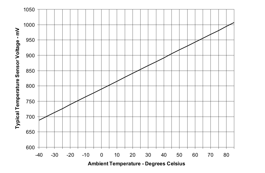 Figure 4-11 Typical Temperature Sensor Voltage
4.34 Comparator_D
over operating free-air temperature range (unless otherwise noted)| PARAMETER | TEST CONDITIONS | MIN | TYP | MAX | UNIT | |
|---|---|---|---|---|---|---|
| tpd | Propagation delay, AVCC = 2 V to 3.6 V |
Overdrive = 10 mV, VIN- = (VIN+ – 400 mV) to (VIN+ + 10 mV) |
49 | 100 | 202 | ns |
| Overdrive = 100 mV, VIN- = (VIN+ – 400 mV) to (VIN+ + 100 mV) |
80 | ns | ||||
| Overdrive = 250 mV, (VIN+ – 400 mV) to (VIN+ + 250 mV) |
50 | ns | ||||
| tfilter | Filter timer added to the propagation delay of the comparator | CDF = 1, CDFDLY = 00 | 0.28 | 0.5 | 1.1 | µs |
| CDF = 1, CDFDLY = 01 | 0.49 | 0.9 | 1.8 | µs | ||
| CDF = 1, CDFDLY = 10 | 0.85 | 1.6 | 3.31 | µs | ||
| CDF = 1, CDFDLY = 11 | 1.59 | 3.0 | 6.5 | µs | ||
| Voffset | Input offset | AVCC = 2 V to 3.6 V | –26 | 26 | mV | |
| Vic | Common mode input range | AVCC = 2 V to 3.6 V | 0 | AVCC – 1 | V | |
| Icomp(AVCC) | Comparator only | CDON = 1, AVCC = 2 V to 3.6 V | 28 | µA | ||
| Iref(AVCC) | Reference buffer and R-ladder | CDREFLx = 01, AVCC = 2 V to 3.6 V | 20 | µA | ||
| tenable,comp | Comparator enable time | CDON = 0 to CDON = 1, AVCC = 2 V to 3.6 V |
1.1 | 2.3 | µs | |
| tenable,rladder | Resistor ladder enable time | CDON = 0 to CDON = 1, AVCC = 2 V to 3.6 V |
1.1 | 2.3 | µs | |
| VCB_REF | Reference voltage for a tap | VIN = voltage input to the R-ladder, n = 0 to 31 |
VIN × (n + 0.49) / 32 |
VIN × (n + 1) / 32 |
VIN × (n + 1.51) / 32 |
V |
4.35 FRAM
over recommended ranges of supply voltage and operating free-air temperature (unless otherwise noted)| PARAMETER | TEST CONDITIONS | MIN | TYP | MAX | UNIT | |
|---|---|---|---|---|---|---|
| DVCC(WRITE) | Write supply voltage | 2.0 | 3.6 | V | ||
| tWRITE | Word or byte write time | 120 | ns | |||
| tACCESS | Read access time (1) | 60 | ns | |||
| tPRECHARGE | Precharge time (1) | 60 | ns | |||
| tCYCLE | Cycle time, read or write operation (1) | 120 | ns | |||
| Read and write endurance | 1015 | cycles | ||||
| tRetention | Data retention duration | TJ = 25°C | 100 | years | ||
| TJ = 70°C | 40 | |||||
| TJ = 85°C | 10 | |||||
(1) When using manual wait state control, see the MSP430FR57xx Family User's Guide (SLAU272) for recommended settings for common system frequencies.
4.36 JTAG and Spy-Bi-Wire Interface
over recommended ranges of supply voltage and operating free-air temperature (unless otherwise noted)| PARAMETER | VCC | MIN | TYP | MAX | UNIT | |
|---|---|---|---|---|---|---|
| ƒSBW | Spy-Bi-Wire input frequency | 2 V, 3 V | 0 | 20 | MHz | |
| tSBW,Low | Spy-Bi-Wire low clock pulse duration | 2 V, 3 V | 0.025 | 15 | µs | |
| tSBW, En | Spy-Bi-Wire enable time (TEST high to acceptance of first clock edge) (1) | 2 V, 3 V | 1 | µs | ||
| tSBW,Rst | Spy-Bi-Wire return to normal operation time | 18 | 37 | µs | ||
| ƒTCK | TCK input frequency, 4-wire JTAG (2) | 2 V | 0 | 5 | MHz | |
| 3 V | 0 | 10 | MHz | |||
| Rinternal | Internal pulldown resistance on TEST | 2 V, 3 V | 19 | 35 | 51.5 | kΩ |
(1) Tools accessing the Spy-Bi-Wire interface must wait for the tSBW,En time after pulling the TEST/SBWTCK pin high before applying the first SBWTCK clock edge.
(2) ƒTCK may be restricted to meet the timing requirements of the module selected.