JAJSCO9B December 2016 – November 2017 OPA170-Q1 , OPA2170-Q1 , OPA4170-Q1
PRODUCTION DATA.
7 Detailed Description
7.1 Overview
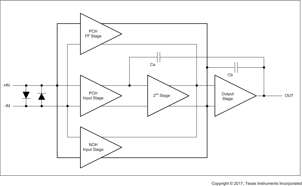
The OPAx170-Q1 family of operational amplifiers provides high overall performance, making them ideal for many general-purpose applications. The excellent offset drift of only 2 μV/°C provides excellent stability over the entire temperature range. In addition, the device offers very good overall performance with high CMRR, PSRR, and AOL.
7.2 Functional Block Diagram
7.3 Feature Description
7.3.1 Operating Characteristics
The OPAx170-Q1 family of amplifiers is specified for operation from 2.7 V to 36 V (±1.35 V to ±18 V). Many of the specifications apply from –40°C to +125°C. Parameters that can exhibit significant variance with regard to operating voltage or temperature are listed in Table 4.
7.3.2 Phase-Reversal Protection
The OPAx170-Q1 family has an internal phase-reversal protection. Many operational amplifiers exhibit a phase reversal when the input is driven beyond the linear common-mode range. This condition is most often encountered in noninverting circuits when the input is driven beyond the specified common-mode voltage range, causing the output to reverse into the opposite rail. The input of the OPAx170-Q1 prevents phase reversal with excessive common-mode voltage. Instead, the output limits into the appropriate rail. Figure 37 shows this performance.
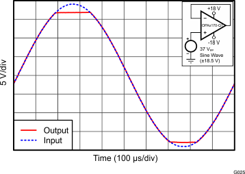 Figure 37. No Phase Reversal
7.3.3 Electrical Overstress
Designers typically ask questions about the capability of an operational amplifier to withstand electrical overstress. These questions typically focus on the device inputs, but may involve the supply voltage pins or the output pin. Each of these different pin functions have electrical stress limits determined by the voltage breakdown characteristics of the particular semiconductor fabrication process and specific circuits connected to the pin. Internal electrostatic discharge (ESD) protection is built into these circuits to protect them from accidental ESD events both before and during product assembly.
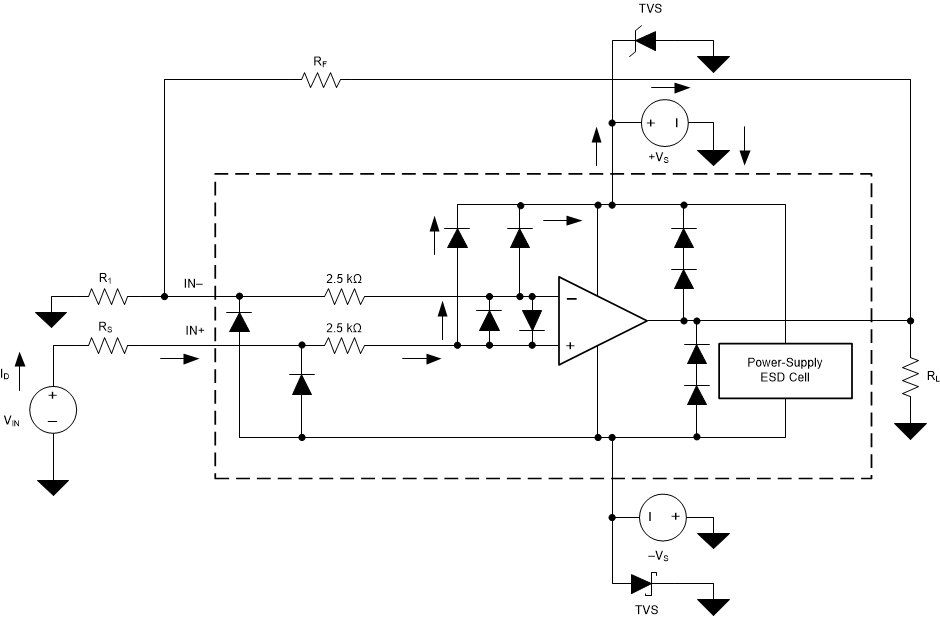
A good understanding of basic ESD circuitry and the relevance of the circuitry to an electrical overstress event is helpful. Figure 38 shows the ESD circuits (indicated by the dashed line area) in the OPAx170-Q1. The ESD protection circuitry involves several current-steering diodes connected from the input and output pins and routed back to the internal power-supply lines, where the diodes meet at an absorption device internal to the operational amplifier. This protection circuitry is intended to remain inactive during normal circuit operation.
An ESD event produces a short-duration, high-voltage pulse that is transformed into a short-duration, high-current pulse when discharging through a semiconductor device. The ESD protection circuits are designed to provide a current path around the operational amplifier core to prevent damage. The energy absorbed by the protection circuitry is then dissipated as heat.
When an ESD voltage develops across two or more amplifier device pins, current flows through one or more steering diodes. The absorption device can activate depending on the path of the current. The absorption device has a trigger (or threshold voltage) that is above the normal operating voltage of the OPAx170-Q1, but below the device breakdown voltage level. When this threshold is exceeded, the absorption device quickly activates and clamps the voltage across the supply rails to a safe level.
When the operational amplifier connects into a circuit (see Figure 38), the ESD protection components are intended to remain inactive and do not become involved in the application circuit operation. However, circumstances may arise where an applied voltage exceeds the operating voltage range of a given pin. If this condition occurs, there is a risk that some internal ESD protection circuits can turn on and conduct current. Any such current flow occurs through steering-diode paths and rarely involves the absorption device.
Figure 38 shows a specific example where the input voltage (VIN) exceeds the positive supply voltage (V+) by 500 mV or more. Much of what happens in the circuit depends on the supply characteristics. If V+ can sink the current, one of the upper input steering diodes conducts and directs current to V+. Excessively high current levels can flow with increasingly higher VIN. As a result, the data sheet specifications recommend that applications limit the input current to 10 mA.
If the supply is not capable of sinking the current, VIN can begin sourcing current to the operational amplifier and then take over as the source of positive supply voltage. The danger in this case is that the voltage can rise to levels that exceed the operational amplifier absolute maximum ratings.
Another common question involves what happens to the amplifier if an input signal is applied to the input when the power supplies (V+ or V–) are at 0 V. Again, this question depends on the supply characteristic when at 0 V, or at a level below the input signal amplitude. If the supplies appear as high impedance, then the input source supplies the operational amplifier current through the current-steering diodes. This state is not a normal bias condition; most likely, the amplifier does not operate normally. If the supplies are low impedance, then the current through the steering diodes can become quite high. The current level depends on the ability of the input source to deliver current, and any resistance in the input path.
If there is any uncertainty about the ability of the supply to absorb this current, add external Zener diodes to the supply pins; see Figure 38. Select the Zener voltage so that the diode does not turn on during normal operation. However, the Zener voltage must be low enough so that the Zener diode conducts if the supply pin begins to rise above the safe-operating, supply-voltage level.
The OPAx170-Q1 input pins are protected from excessive differential voltage with back-to-back diodes, as shown in Figure 38. In most circuit applications, the input protection circuitry has no effect. However, in low-gain or G = 1 circuits, fast-ramping input signals can forward-bias these diodes because the output of the amplifier cannot respond rapidly enough to the input ramp. If the input signal is fast enough to create this forward-bias condition, limit the input signal current to 10 mA or less. If the input signal current is not inherently limited, an input series resistor can limit the input signal current. This input series resistor degrades the low-noise performance of the OPAx170-Q1. Figure 38 is an example configuration that implements a current-limiting feedback resistor.
7.3.4 Capacitive Load and Stability
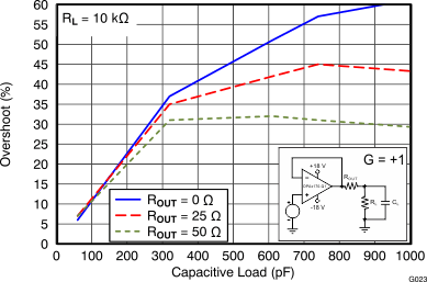
The dynamic characteristics of the OPAx170-Q1 are optimized for common operating conditions. The combination of low closed-loop gain and high capacitive loads decreases the phase margin of the amplifier and can lead to gain peaking or oscillations. As a result, heavier capacitive loads must be isolated from the output. The simplest way to achieve this isolation is to add a small resistor (for example, ROUT equal to 50 Ω) in series with the output. Figure 39 and Figure 40 are graphs showing small-signal overshoot versus capacitive load for several values of ROUT. See Feedback Plots Define Op Amp AC Performance for details of analysis techniques and application circuits.
| 100-mV output step | G = 1 |
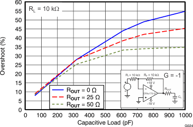
| 100-mV output step | G = –1 |
7.4 Device Functional Modes
7.4.1 Common-Mode Voltage Range
The input common-mode voltage range of the OPAx170-Q1 series extends 100 mV below the negative rail and within 2 V of the top rail for normal operation.
This device can operate with full rail-to-rail input 100 mV beyond the top rail, but with reduced performance within 2 V of the top rail. The typical performance in this range is summarized in Table 5.
Table 5. Typical Performance for Common-Mode Voltages Within 2 V of the Positive Supply
| PARAMETER | MIN | TYP | MAX | UNIT | |
|---|---|---|---|---|---|
| Input common-mode voltage | (V+) – 2 | (V+) + 0.1 | V | ||
| Offset voltage | 7 | mV | |||
| vs temperature | 12 | µV/°C | |||
| Common-mode rejection | 65 | dB | |||
| Open-loop gain | 60 | dB | |||
| Gain-bandwidth product | 0.3 | MHz | |||
| Slew rate | 0.3 | V/µs | |||
7.4.2 Overload Recovery
Overload recovery is defined as the time required for the operational amplifier output to recover from the saturated state to the linear state. The output devices of the operational amplifier enter the saturation region when the output voltage exceeds the rated operating voltage, either resulting from the high input voltage or the high gain. After the device enters the saturation region, the charge carriers in the output devices need time to return back to the normal state. After the charge carriers return back to the equilibrium state, the device begins to slew at the normal slew rate. Thus, the propagation delay in case of an overload condition is the sum of the overload recovery time and the slew time. The overload recovery time for the OPAx170-Q1 is approximately 2 µs.
