JAJSE33A November 2017 – December 2017 OPA2333P
PRODUCTION DATA.
- 1 特長
- 2 アプリケーション
- 3 概要
- 4 改訂履歴
- 5 Pin Configuration and Functions
- 6 Specifications
- 7 Detailed Description
- 8 Application and Implementation
- 9 Power Supply Recommendations
- 10Layout
- 11デバイスおよびドキュメントのサポート
- 12メカニカル、パッケージ、および注文情報
パッケージ・オプション
メカニカル・データ(パッケージ|ピン)
- DSG|8
サーマルパッド・メカニカル・データ
- DSG|8
発注情報
6.6 Typical Characteristics
Table 1. List of Typical Characteristics
| TITLE | FIGURE |
|---|---|
| Offset Voltage Production Distribution | Figure 1 |
| Offset Voltage Drift Production Distribution | Figure 2 |
| Quiescent Current Production Distribution | Figure 3 |
| Open-Loop Gain vs Frequency | Figure 4 |
| Common-Mode Rejection Ratio vs Frequency | Figure 5 |
| Power-Supply Rejection Ratio vs Frequency | Figure 6 |
| Output Voltage Swing vs Output Current | Figure 7 |
| Input Bias Current vs Common-Mode Voltage | Figure 8 |
| Input Bias Current vs Temperature | Figure 9 |
| Quiescent Current vs Temperature | Figure 10 |
| Large-Signal Step Response | Figure 11 |
| Small-Signal Step Response | Figure 12 |
| Positive Overvoltage Recovery | Figure 13 |
| Negative Overvoltage Recovery | Figure 14 |
| Settling Time vs Closed-Loop Gain | Figure 15 |
| Small-Signal Overshoot vs Load Capacitance | Figure 16 |
| 0.1-Hz to 10-Hz Noise | Figure 17 |
| Current and Voltage Noise Spectral Density vs Frequency | Figure 18 |
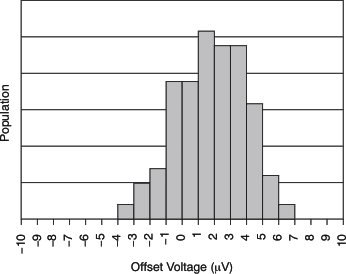
Figure 1. Offset Voltage Production Distribution
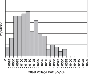
Figure 2. Offset Voltage Drift Production Distribution
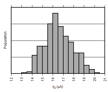
| VS = 5.5 V |
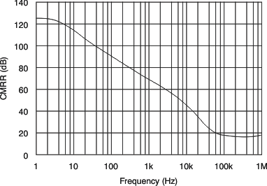
Figure 5. Common-Mode Rejection Ratio vs Frequency
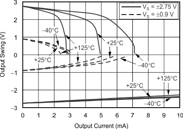
Figure 7. Output Voltage Swing vs Output Current
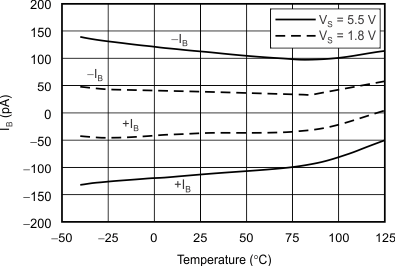
Figure 9. Input Bias Current vs Temperature
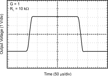
Figure 11. Large-Signal Step Response
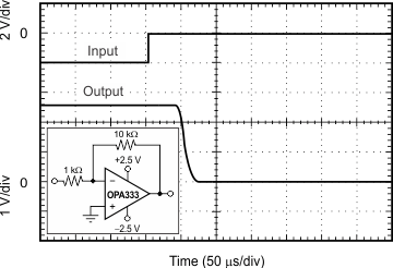
Figure 13. Positive Overvoltage Recovery
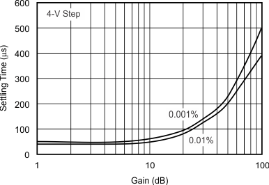
Figure 15. Settling Time vs Closed-Loop Gain
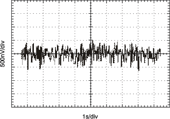
Figure 17. 0.1-Hz to 10-Hz Noise
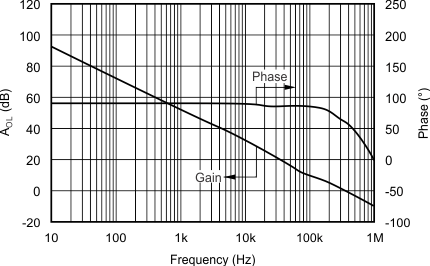
Figure 4. Open-Loop Gain and Phase vs Frequency
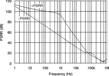
Figure 6. Power-Supply Rejection Ratio vs Frequency
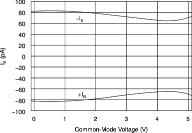
Figure 8. Input Bias Current vs Common-Mode Voltage
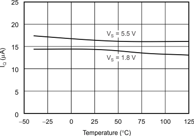
Figure 10. Quiescent Current vs Temperature
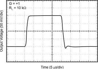
Figure 12. Small-Signal Step Response
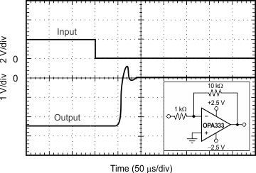
Figure 14. Negative Overvoltage Recovery
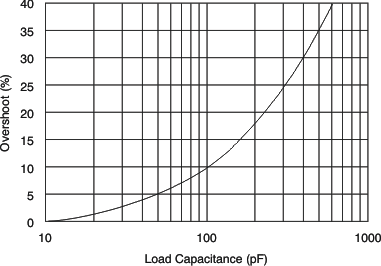
Figure 16. Small-Signal Overshoot
vs Load Capacitance
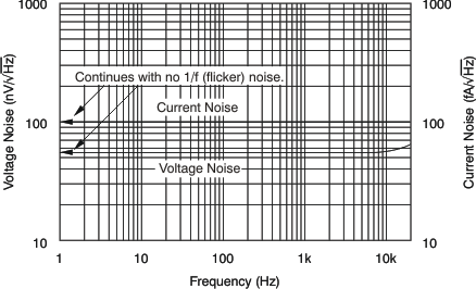
Figure 18. Current and Voltage Noise Spectral Density vs Frequency