JAJSFT1E August 2011 – April 2018 OPA170 , OPA2170 , OPA4170
PRODUCTION DATA.
- 1 特長
- 2 アプリケーション
- 3 概要
- 4 改訂履歴
- 5 Device Comparison Table
- 6 Pin Configuration and Functions
- 7 Specifications
- 8 Detailed Description
- 9 Application and Implementation
- 10Power Supply Recommendations
- 11Layout
- 12デバイスおよびドキュメントのサポート
- 13メカニカル、パッケージ、および注文情報
パッケージ・オプション
メカニカル・データ(パッケージ|ピン)
サーマルパッド・メカニカル・データ
- D|14
発注情報
7.8 Typical Characteristics
VS = ±18 V, VCM = VS / 2, RLOAD = 10 kΩ connected to VS / 2, and CL = 100 pF, (unless otherwise noted)Table 1. Characteristic Performance Measurements
| DESCRIPTION | FIGURE |
|---|---|
| Offset Voltage Production Distribution | Figure 1 |
| Offset Voltage Drift Distribution | Figure 2 |
| Offset Voltage vs Temperature | Figure 3 |
| Offset Voltage vs Common-Mode Voltage | Figure 4 |
| Offset Voltage vs Common-Mode Voltage (Upper Stage) | Figure 5 |
| Offset Voltage vs Power Supply | Figure 6 |
| IB and IOS vs Common-Mode Voltage | Figure 7 |
| Input Bias Current vs Temperature | Figure 8 |
| Output Voltage Swing vs Output Current (Maximum Supply) | Figure 9 |
| CMRR and PSRR vs Frequency (Referred-to-Input) | Figure 10 |
| CMRR vs Temperature | Figure 11 |
| PSRR vs Temperature | Figure 12 |
| 0.1-Hz to 10-Hz Noise | Figure 13 |
| Input Voltage Noise Spectral Density vs Frequency | Figure 14 |
| THD+N Ratio vs Frequency | Figure 15 |
| THD+N vs Output Amplitude | Figure 16 |
| Quiescent Current vs Temperature | Figure 17 |
| Quiescent Current vs Supply Voltage | Figure 18 |
| Open-Loop Gain and Phase vs Frequency | Figure 19 |
| Closed-Loop Gain vs Frequency | Figure 20 |
| Open-Loop Gain vs Temperature | Figure 21 |
| Open-Loop Output Impedance vs Frequency | Figure 22 |
| Small-Signal Overshoot vs Capacitive Load (100-mV Output Step) | Figure 23, Figure 24 |
| No Phase Reversal | Figure 25 |
| Positive Overload Recovery | Figure 26 |
| Negative Overload Recovery | Figure 27 |
| Small-Signal Step Response (100 mV) | Figure 28, Figure 29 |
| Large-Signal Step Response | Figure 30, Figure 31 |
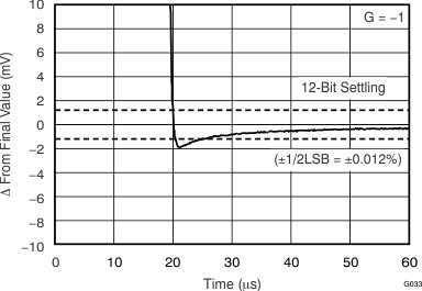
| Large-Signal Settling Time (10-V Positive Step) | Figure 32 |
| Large-Signal Settling Time (10-V Negative Step) | Figure 33 |
| Short-Circuit Current vs Temperature | Figure 34 |
| Maximum Output Voltage vs Frequency | Figure 35 |
| EMIRR IN+ vs Frequency | Figure 36 |
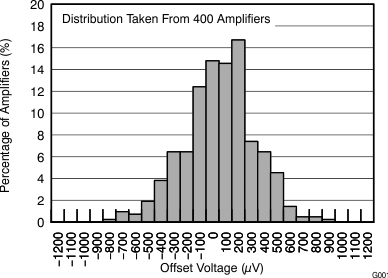 Figure 1. Offset Voltage Production Distribution
 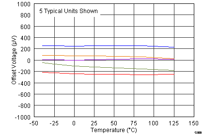 Figure 3. Offset Voltage vs Temperature
 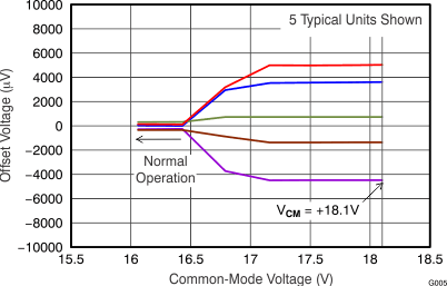 Figure 5. Offset Voltage vs Common-Mode Voltage
(Upper Stage)
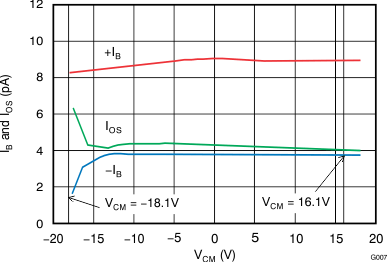 Figure 7. IB and IOS vs Common-Mode Voltage
 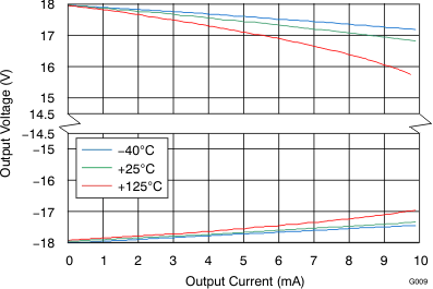 Figure 9. Output Voltage Swing vs Output Current (Maximum Supply)
 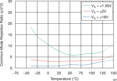 Figure 11. CMRR vs Temperature
 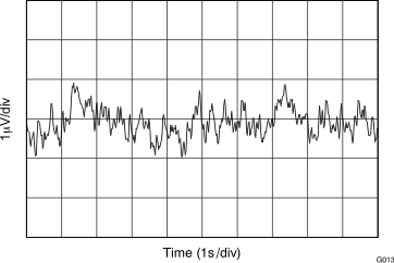 Figure 13. 0.1-Hz to 10-Hz Noise
 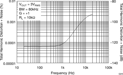 Figure 15. THD+N Ratio vs Frequency
 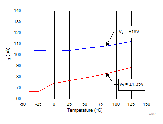 Figure 17. Quiescent Current vs Temperature
 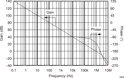 Figure 19. Open-Loop Gain and Phase vs Frequency
 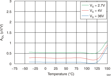 Figure 21. Open-Loop Gain vs Temperature
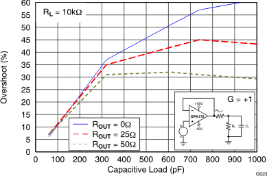
| 100-mV output step |
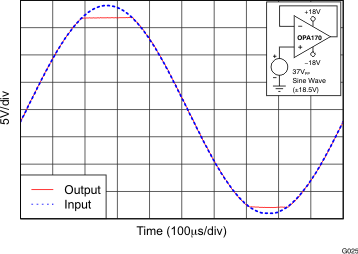 Figure 25. No Phase Reversal
 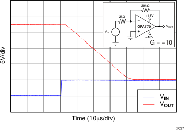 Figure 27. Negative Overload Recovery
 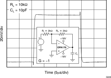 Figure 29. Small-Signal Step Response (100 mV)
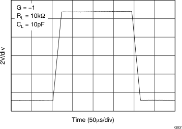
A.
Figure 33. Large-Signal Settling Time | 10-V negative step |
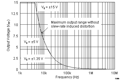 Figure 35. Maximum Output Voltage vs Frequency
 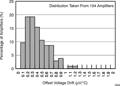 Figure 2. Offset Voltage Drift Distribution
 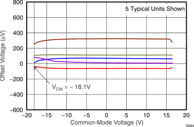 Figure 4. Offset Voltage vs Common-Mode Voltage
 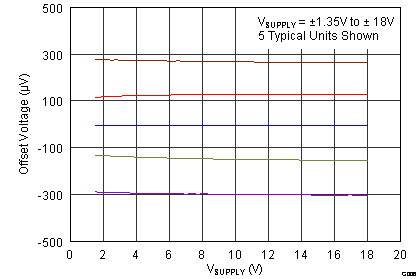 Figure 6. Offset Voltage vs Power Supply
 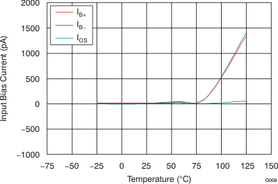 Figure 8. Input Bias Current vs Temperature
 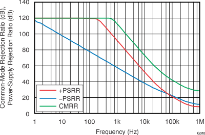 Figure 10. CMRR and PSRR vs Frequency
(Referred-to Input)
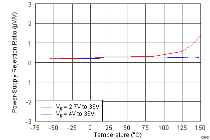 Figure 12. PSRR vs Temperature
 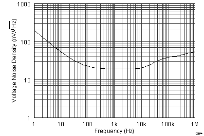 Figure 14. Input Voltage Noise Spectral Density vs Frequency
 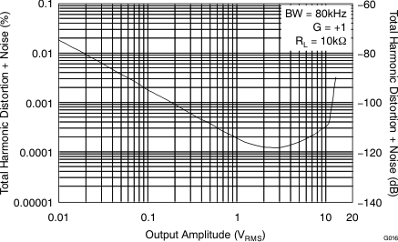 Figure 16. THD+N vs Output Amplitude
 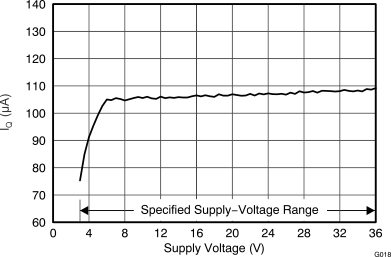 Figure 18. Quiescent Current vs Supply Voltage
 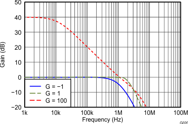 Figure 20. Closed-Loop Gain vs Frequency
 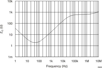 Figure 22. Open-Loop Output Impedance vs Frequency
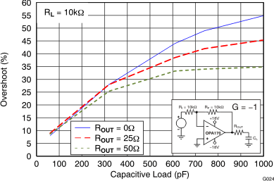
| 100-mV output step |
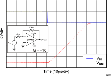 Figure 26. Positive Overload Recovery
 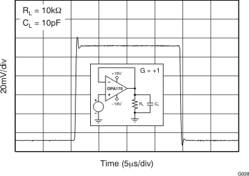 Figure 28. Small-Signal Step Response (100 mV)
 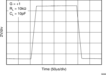 Figure 30. Large-Signal Step Response
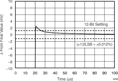
| 10-V positive step |
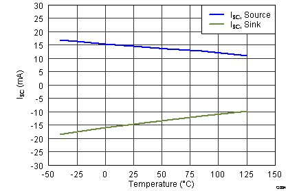
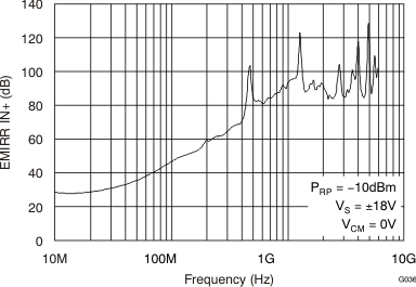 Figure 36. EMIRR IN+ vs Frequency