JAJSC13F September 2003 – September 2016 OPA2373 , OPA2374 , OPA373 , OPA374 , OPA4374
PRODUCTION DATA.
- 1 特長
- 2 アプリケーション
- 3 概要
- 4 改訂履歴
- 5 Device Comparison Table
- 6 Pin Configuration and Functions
-
7 Specifications
- 7.1 Absolute Maximum Ratings
- 7.2 ESD Ratings
- 7.3 Recommended Operating Conditions
- 7.4 Thermal Information: OPA373
- 7.5 Thermal Information: OPA374
- 7.6 Thermal Information: OPA2373
- 7.7 Thermal Information: OPA2374
- 7.8 Thermal Information: OPA4374
- 7.9 Electrical Characteristics: VS = 2.7 V to 5.5 V
- 7.10 Typical Characteristics
- 8 Detailed Description
- 9 Application and Implementation
- 10Power Supply Recommendations
- 11Layout
- 12デバイスおよびドキュメントのサポート
- 13メカニカル、パッケージ、および注文情報
パッケージ・オプション
メカニカル・データ(パッケージ|ピン)
サーマルパッド・メカニカル・データ
- PW|14
発注情報
9 Application and Implementation
NOTE
Information in the following applications sections is not part of the TI component specification, and TI does not warrant its accuracy or completeness. TI’s customers are responsible for determining suitability of components for their purposes. Customers should validate and test their design implementation to confirm system functionality.
9.1 Application Information
The OPA373 and OPA374 series op amps are unity-gain stable and suitable for a wide range of general-purpose applications. Rail-to-rail input and output make them ideal for driving sampling analog-to-digital converters (ADCs). Excellent AC performance makes them well-suited for audio applications. The class AB output stage is capable of driving 100-kΩ loads connected to any point between V+ and ground.
The input common-mode voltage range includes both rails, allowing the OPA373 and OPA374 series op amps to be used in virtually any single-supply application up to a supply voltage of 5.5 V. Rail-to-rail input and output swing significantly increases dynamic range, especially in low-supply applications. Power-supply pins must be bypassed with 0.01-µF ceramic capacitors.
9.2 Typical Application
This single-supply, low-side, bidirectional current-sensing solution detects load currents from –1 A to 1 A. The single-ended output spans from 110 mV to 3.19 V. This design uses the OPA2374 because of its rail-to-rail input and output range and cost compared to performance. One of the amplifiers is configured as a difference amplifier, and the other amplifier provides the reference voltage.
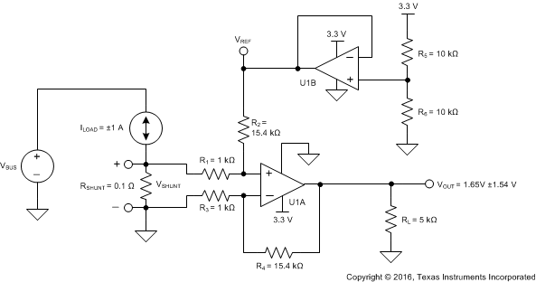 Figure 27. Single-Supply, Low-Side, Bidirectional Current-Sensing Solution
9.2.1 Design Requirements
This design has the following requirements:
- Supply voltage: 3.3 V
- Input: –1 A to 1 A
- Output: 1.65 V ±1.54 V (110 mV to 3.19 V)
9.2.2 Detailed Design Procedure
The load current, ILOAD, flows through the shunt resistor (RSHUNT) to develop the shunt voltage, VSHUNT. The shunt voltage is then amplified by the difference amplifier, which consists of U1A and R1 through R4. The gain of the difference amplifier is set by the ratio of R4 to R3. To minimize errors, set R2 = R4 and R1 = R3. The reference voltage, VREF, is supplied by buffering a resistor divider using U1B. The transfer function is given by Equation 1.

where
There are two types of errors in this design: offset and gain. Gain errors are introduced by the tolerance of the shunt resistor and the ratios of R4 to R3 and, similarly, R2 to R1. Offset errors are introduced by the voltage divider (R5 and R6) and how closely the ratio of R4/R3 matches the ratio of R2/R1. The ratio of R2/R1 impacts the CMRR of the difference amplifier, which ultimately translates to an offset error.
This is a low-side measurement. Therefore, the value of VSHUNT is the ground potential for the system load. Thus, it is important to place a maximum value on VSHUNT. In this design, the maximum value for VSHUNT is set to 100 mV. Equation 2 calculates the maximum value of the shunt resistor given a maximum shunt voltage of
100 mV and maximum load current of 1 A.

The tolerance of RSHUNT is directly proportional to cost. For this design, a shunt resistor with a tolerance of 0.5% was selected. If greater accuracy is required, select a 0.1% resistor or better.
Because the load current is bidirectional, the shunt voltage range is –100 mV to 100 mV. This voltage is divided down by R1 and R2 before reaching the op amp, U1A. Take care to ensure that the voltage present at the noninverting node of U1A is within the common-mode range of the device.
It is therefore important to use an op amp, such as the OPA374, that has a common-mode range that extends below the negative supply voltage.
Given a symmetric load current of –1 A to 1 A, the voltage divider resistors (R5 and R6) must be equal. To be consistent with the shunt resistor, a tolerance of 0.5% was selected. To minimize power consumption,
10-kΩ resistors were used.
To set the gain of the difference amplifier, the common-mode range and output swing of the OPA374 must be considered. Equation 3 and Equation 4 depict the typical common-mode range and output swing of the OPA374, given a 3.3-V supply.
The gain of the difference amplifier can now be calculated as shown in Equation 5.

The resistor value selected for R1 and R3 was 1 kΩ. 15.4 kΩ was selected for R2 and R4 because it is the nearest standard value. Therefore, the ideal gain of the difference amplifier is 15.4V/V.
Because the gain error of the circuit primarily depends on R1 through R4, 0.1% resistors were selected. This value reduces the likelihood that the design requires a two-point calibration. A simple one-point calibration, if desired, removes the offset errors introduced by the 0.5% resistors.
9.2.3 Application Curve
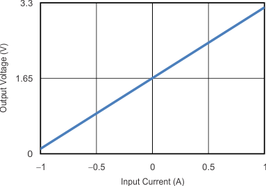 Figure 28. Output Voltage vs Input Current
9.3 System Examples
9.3.1 Driving ADCs
The OPA373 and OPA374 series op amps are optimized for driving medium-speed sampling ADCs. The OPA373 and OPA374 op amps buffer the ADC input capacitance and resulting charge injection, while providing signal gain.
The OPA373 is shown driving the ADS7816 in a basic noninverting configuration, as Figure 29 shows. The ADS7816 is a 12-bit, MicroPower sampling converter in the 8-pin VSSOP package. When used with the low-power, miniature packages of the OPA373, the combination is ideal for space-limited, low-power applications. In this configuration, an RC network at the ADC input can be used to provide anti-aliasing filtering.
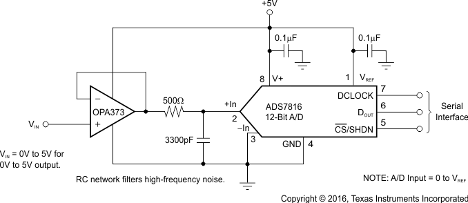 Figure 29. The OPA373 in Noninverting Configuration Driving the ADS7816
Figure 30 shows the OPA373 driving the ADS7816 in a speech bypass-filtered data acquisition system. This small, low-cost solution provides the necessary amplification and signal conditioning to interface directly with an electret microphone. This circuit operates with VS = 2.7 V to 5 V.
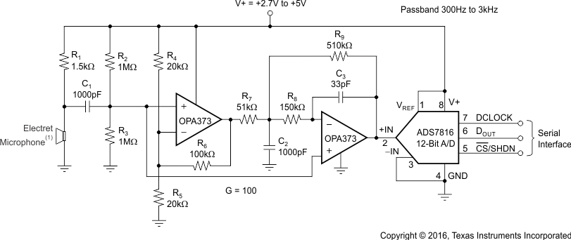 Figure 30. The OPA2373 as a Speech Bypass-Filtered Data Acquisition System
The OPA373 is shown in the inverting configuration described in Figure 31. In this configuration, filtering may be accomplished with the capacitor across the feedback resistor.
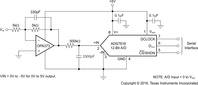 Figure 31. The OPA373 in Inverting Configuration Driving the ADS7816
Figure 32 shows the OPA373 configured as a three-pole, Sallen-Key, Butterworth low-pass filter.
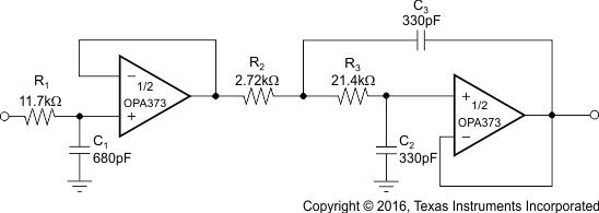 Figure 32. Three-Pole, Sallen-Key, Butterworth Low-Pass Filter


