JAJSC13F September 2003 – September 2016 OPA2373 , OPA2374 , OPA373 , OPA374 , OPA4374
PRODUCTION DATA.
- 1 特長
- 2 アプリケーション
- 3 概要
- 4 改訂履歴
- 5 Device Comparison Table
- 6 Pin Configuration and Functions
-
7 Specifications
- 7.1 Absolute Maximum Ratings
- 7.2 ESD Ratings
- 7.3 Recommended Operating Conditions
- 7.4 Thermal Information: OPA373
- 7.5 Thermal Information: OPA374
- 7.6 Thermal Information: OPA2373
- 7.7 Thermal Information: OPA2374
- 7.8 Thermal Information: OPA4374
- 7.9 Electrical Characteristics: VS = 2.7 V to 5.5 V
- 7.10 Typical Characteristics
- 8 Detailed Description
- 9 Application and Implementation
- 10Power Supply Recommendations
- 11Layout
- 12デバイスおよびドキュメントのサポート
- 13メカニカル、パッケージ、および注文情報
パッケージ・オプション
メカニカル・データ(パッケージ|ピン)
サーマルパッド・メカニカル・データ
- PW|14
発注情報
11 Layout
11.1 Layout Guidelines
The leadframe die pad must be soldered to a thermal pad on the PCB. A mechanical data sheet showing an example layout is attached at the end of this data sheet. Refinements to this layout may be required based on assembly process requirements.
Mechanical drawings located at the end of this data sheet list the physical dimensions for the package and pad. The five holes in the landing pattern are optional, and are intended for use with thermal vias that connect the leadframe die pad to the heat sink area on the PCB. Soldering the exposed pad significantly improves board-level reliability during temperature cycling, key push, package shear, and similar board-level tests.
Even with applications that have low-power dissipation, the exposed pad must be soldered to the PCB to provide structural integrity and long-term reliability.
11.1.1 VSON Package
The OPA2373 is available in a 10-pin VSON package, which is a VQFN package with lead contacts on only two sides of the bottom of the package. This leadless, near-chip-scale package maximizes board space and enhances thermal and electrical characteristics through an exposed pad. VSON packages are physically small, have a smaller routing area, improved thermal performance, and improved electrical parasitics, with a pinout scheme that is consistent with other commonly-used packages, such as SOIC and VSSOP. Additionally, the absence of external leads eliminates bent-lead issues.
The VSON package can be easily mounted using standard PCP assembly techniques. See QFN/SON PCB Attachment and Quad Flatpack No-Lead Logic Packages, both available for download at www.ti.com.
NOTE
The exposed leadframe die pad on the bottom of the package must be connected to V−.
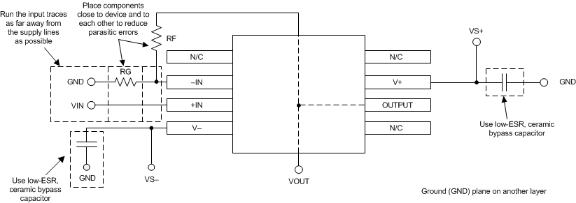
11.2 Layout Example
 Figure 33. Operational Amplifier Board Layout for Noninverting Configuration