SBOS688A April 2015 – October 2015 OPA2625 , OPA625
PRODUCTION DATA.
- 1 Features
- 2 Applications
- 3 Description
- 4 Revision History
- 5 Pin Configuration and Functions
-
6 Specifications
- 6.1 Absolute Maximum Ratings
- 6.2 ESD Ratings
- 6.3 Recommended Operating Conditions
- 6.4 Thermal Information
- 6.5 Electrical Characteristics High-Drive Mode
- 6.6 Electrical Characteristics Low-Power Mode
- 6.7 Electrical Characteristics High-Drive Mode
- 6.8 Electrical Characteristics Low-Power Mode
- 6.9 Switching Characteristics
- 6.10 Typical Characteristics
- 7 Parameter Measurement Information
- 8 Detailed Description
- 9 Application and Implementation
- 10Power Supply Recommendations
- 11Layout
- 12Device and Documentation Support
- 13Mechanical, Packaging, and Orderable Information
7 Parameter Measurement Information
7.1 DC Parameter Measurements
The circuit shown in Figure 64 is used to measure the dc input offset related parameters of the OPAx625. Input offset voltage, power supply rejection ratio, common mode rejection ratio and open loop gain can be measured with this circuit. The basic test procedure requires setting the inputs (the power-supply voltage, VS, and the common-mode voltage, VCM), to the desired values. VO is set to the desired value by adjusting the loop-drive voltage while measuring VO. After all inputs are configured, measure the input offset at the VX measurement point. Calculate the input offset voltage by dividing the measured result by 101. Changing the voltages on the various inputs changes the input offset voltage. The input parameters can be measured according to the relationships illustrated in Equation 1 through Equation 5.
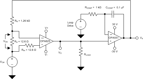 Figure 64. DC-Parameters Measurement Circuit


7.2 Transient Parameter Measurements
The circuit shown in Figure 65 is used to measure the transient response of the OPAx625. Configure V+, V–, RISO, RLOAD, and CLOAD as desired. Monitor the input and output voltages on an oscilloscope or other signal analyzer. Use this circuit to measure large-signal and small-signal transient response, slew rate, overshoot, and capacitive-load stability.
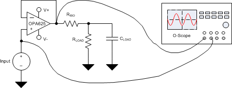 Figure 65. Pulse-Response Measurement Circuit
7.3 AC Parameter Measurements
The circuit shown in Figure 66 is used to measure the ac parameters of the OPAx625. Configure V+, V–, and CLOAD as desired. The THS4271 are used to buffer the input and output of the OPAx625 to prevent loading by the gain phase analyzer. Monitor the input and output voltages on a gain phase analyzer. Use this circuit to measure the gain bandwidth product, and open-loop gain versus frequency versus capacitive load.
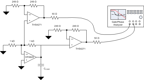 Figure 66. AC-Parameters Measurement Circuit
7.4 Noise Parameter Measurements
The circuit shown in Figure 67 is used to measure the voltage noise of the OPAx625. Configure V+, V–, and CLOAD as desired.
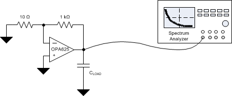 Figure 67. Voltage Noise Measurement Circuit
The circuit shown in Figure 68 is used to measure the current noise of the OPAx625. Configure V+, V– and CLOAD as desired.
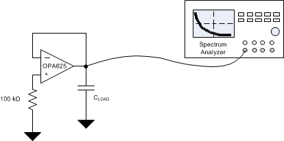 Figure 68. Current Noise Measurement Circuit
The circuit shown in Figure 69 is used to measure the OPAx625 0.1-Hz to 10-Hz voltage noise. Configure V+, V–, and CLOAD as desired.
 Figure 69. 0.1-Hz to 10-Hz Voltage-Noise Measurement Circuit