SBOS630D December 2013 – August 2016 OPA857
PRODUCTION DATA.
- 1 Features
- 2 Applications
- 3 Description
- 4 Revision History
- 5 Pin Configuration and Functions
- 6 Specifications
- 7 Detailed Description
- 8 Application and Implementation
- 9 Power-Supply Recommendations
- 10Layout
- 11Device and Documentation Support
- 12Mechanical, Packaging, and Orderable Information
パッケージ・オプション
メカニカル・データ(パッケージ|ピン)
- RGT|16
サーマルパッド・メカニカル・データ
- RGT|16
発注情報
8 Application and Implementation
NOTE
Information in the following applications sections is not part of the TI component specification, and TI does not warrant its accuracy or completeness. TI’s customers are responsible for determining suitability of components for their purposes. Customers should validate and test their design implementation to confirm system functionality.
8.1 Application Information
The OPA857 is a transimpedance amplifier offering two selectable gains. This device is used in conjunction with a photodiode at its input. The output is pseudo differential and may or may not require the use of a fully differential amplifier, depending on the analog-to-digital converter (ADC) used for implementation.
The OPA857 requires a photodiode to be connected to the positive bias voltage because the output voltage can only swing down from the reference voltage (1.85 V for a 3.3-V supply) to ground.
8.2 Typical Application
8.2.1 TIA With Associated Signal Chain
Figure 39 presents a complete end-to-end receive signal chain for an optical input. It includes a high-speed photodiode, the OPA857, a THS4541 fully-differential amplifier, and a 16-bit, 160-MSPS, high-speed ADC. For the complete wide-bandwidth, optical front-end reference design, go to http://www.ti.com/tool/TIDA-00725.
 Figure 39. TIA With Associated Signal Chain
8.2.1.1 Design Requirements
For this example, use the values listed in Table 3 for the input parameters.
Table 3. Design Parameters
| DESIGN PARAMETER | EXAMPLE VALUE |
|---|---|
| Supply voltage | 5-V external supply |
| Analog bandwidth | 120 MHz |
| ADC sampling rate | 160 MSPS |
| Maximum system gain | 100 kΩ |
| Programmable transimpedance gain | 5 kΩ / 20 kΩ |
| Maximum signal swing | 1 VPP |
| Noise performance | ≥ 60-dB SNR |
| Averaged noise performance | < 10-µVRMS |
8.2.1.2 Detailed Design Procedure
- Use a high-speed, low input capacitance photodiode, such as the NR7500 or NR8300, as the front-end optical sensor. Take care during layout to minimize parasitic capacitance added because of the PCB.
- Bias the photodiode with the cathode connected to a positive supply, and the anode connected to IN pin of the OPA857. These connections make sure that the photodiode sources an output current that results in the OPA857 output swinging down below the reference voltage = (5 / 9) × 3.3 V = 1.83 V.
- Disable the OPA857 test mode by setting Test_IN = +VS and Test_SD = GND. The transimpedance gain is selected by setting CTRL = +VS (gain = 20 kΩ) or CTRL = GND (gain = 5 kΩ).
- The THS4541 is configured in a gain of 5 V/V in order to achieve a maximum signal transimpedance gain of 100 kΩ. It is important to carefully select the value of the RG gain resistors for the THS4541.
- Setting RG very low increases the resistive loading on the previous OPA857 output stage, and reduces the bandwidth of the OPA857.
- Setting RG very high results in a large value of feedback resistance, RF, on the THS4541 in order to achieve the desired 5V/V gain. RF interacts with the input capacitance of the THS4541 to create a zero in the noise-gain response of the amplifier, and if not properly compensated, results in reduced phase-margin and potential instability.
- A value of RG = 374 Ω was selected that results in a total differential load of 798 Ω on the OPA857. The resultant RF = 2 kΩ.
- The response to an optical pulsed input is shown in Figure 40 to Figure 43. To prevent signal reflections between the THS4541 output and the ADC34J45 input, the signal is doubly terminated through 50-Ω resistors. If the THS4541 and ADC34J45 are physically close together on the PCB, then the double-termination is eliminated, which increases the overall gain of the signal chain without affecting the transient response of the system. These results were verified, and the complete data is available in reference design TIDA-00725.
- An optional antialiasing filter can be added between the THS4541 and the ADC34J45 to reduce system noise caused by aliasing.
8.2.1.3 Application Curves
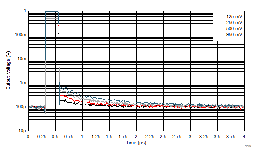
| TZ Gain = 20 kΩ |
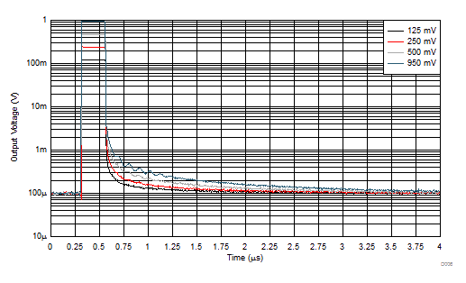
| TZ Gain = 5 kΩ |
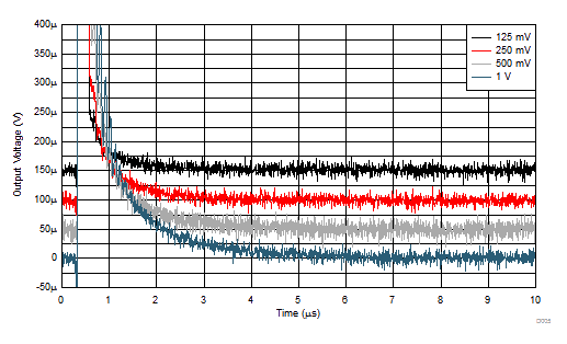
| TZ Gain = 20 kΩ |
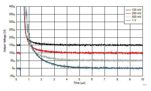
| TZ Gain = 5 kΩ |
8.2.2 Extending Transimpedance Bandwidth
At the core of the OPA857 is an ultrawide bandwidth op amp. One of the highlights of the OPA857 is the relatively small change in the transimpedance bandwidth as a function of the internal gain selected; 130 MHz (gain = 5 kΩ) and 105 MHz (gain = 20 kΩ). Theoretically, for a four times increase in gain, the bandwidth should reduce by two times; however, as observed in the case of the OPA857, the results do not follow theory. For more information on the various factors that contribute to an amplifier frequency-response performance when configured as a TIA, see What You Need To Know About Transimpedance Amplifiers – Part 1 on the TI E2E Community website at e2e.ti.com. This blog also contains a reference to an excel calculator to simplify TIA designs when using discrete opamps. The OPA857 is unique in displaying this type of behavior because the CTRL logic controls an internal switch in the amplifier core that recompensates the amplifier open-loop gain characteristic depending upon the logic level. In this application, it it shown how the closed-loop transimpedance bandwidth can be increased to greater than 250 MHz. The circuit used for this test is shown in Figure 44. An external feedback resistor, RF, is added in parallel to the internal transimpedance gain resistors of the OPA857. This resistor has the effect of reducing the overall transimpedance gain, but with increased bandwidth.
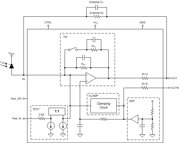 Figure 44. Extending Transimpedance Bandwidth
8.2.2.1 Design Requirements
For this example, use the values listed in Table 4 for the input parameters.
Table 4. Design Parameters
| DESIGN PARAMETER | EXAMPLE VALUE |
|---|---|
| Supply voltage | 3.3 V |
| Output swing | 500 mVPP |
| Differential output load | 500 kΩ and 1 kΩ |
| Target bandwidth | 250 MHz |
| Effective transimpedance gain | 5 kΩ |
8.2.2.2 Application Curves
Figure 45 shows the frequency response with a feedback resistance of 6.8 kΩ and an output load of 500 Ω. The large amount of peaking indicates a low phase-margin and potential instability. Next, a 0.1-pF feedback capacitor, CF, is added in parallel to the 6.8-kΩ RF. Both RF and CF interact to create pole in the noise gain curve that counteracts the effect of the zero caused by RF, and the total input capacitance at pin IN of the OPA857. The input capacitance is caused by the opamps inherent input capacitance, the photodiode capacitance, and the parasitic input capacitance from the PCB. The pole zero cancellation increases the phase margin, as is evident in the reduced peaking shown in Figure 46. In Figure 47, an output load of 1 kΩ was used, along with an RF = 6.8 kΩ and CF = 0.1 pF. The reduced load helps to increase the op amp open-loop gain, which in turn increases the closed-loop bandwidth of the OPA857 circuit.
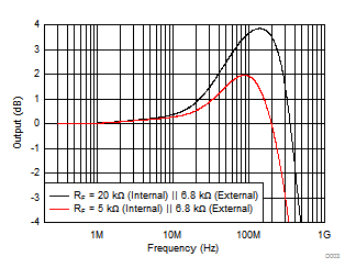
| RF = 6.8 kΩ |
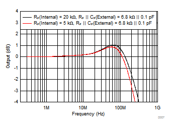
| RF = 6.8 kΩ, CF = 0.1 pF |
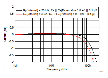
| RF = 6.8 kΩ, CF = 0.1 pF |