SLLS877H December   2007  – March 2017 SN65HVD1780 , SN65HVD1781 , SN65HVD1782

PRODUCTION DATA.  

  1. Features
  2. Applications
  3. Description
  4. Revision History
  5. Device Comparison Table
  6. Pin Configuration and Functions
  7. Specifications
    1. 7.1 Absolute Maximum Ratings
    2. 7.2 ESD Ratings: JEDEC
    3. 7.3 ESD Ratings: IEC
    4. 7.4 Recommended Operating Conditions
    5. 7.5 Thermal Information
    6. 7.6 Electrical Characteristics
    7. 7.7 Power Dissipation Characteristics
    8. 7.8 Switching Characteristics
    9. 7.9 Typical Characteristics
  8. Parameter Measurement Information
    1. 8.1 Equivalent Input Schematic
  9. Detailed Description
    1. 9.1 Overview
    2. 9.2 Functional Block Diagram
    3. 9.3 Feature Description
      1. 9.3.1 70-V Fault Protection
      2. 9.3.2 Receiver Failsafe
      3. 9.3.3 Hot-Plugging
    4. 9.4 Device Functional Modes
  10. 10Application and Implementation
    1. 10.1 Application Information
    2. 10.2 Typical Application
      1. 10.2.1 Design Requirements
        1. 10.2.1.1 Data Rate and Bus Length
        2. 10.2.1.2 Stub Length
        3. 10.2.1.3 Bus Loading
        4. 10.2.1.4 Receiver Failsafe
      2. 10.2.2 Detailed Design Procedure
        1. 10.2.2.1 Custom Design with WEBENCH® Tools
      3. 10.2.3 Application Curve
  11. 11Power Supply Recommendations
  12. 12Layout
    1. 12.1 Layout Guidelines
    2. 12.2 Layout Example
  13. 13Device and Documentation Support
    1. 13.1 Device Support
      1. 13.1.1 Custom Design with WEBENCH® Tools
      2. 13.1.2 Third-Party Products Disclaimer
    2. 13.2 Documentation Support
      1. 13.2.1 Related Documentation
    3. 13.3 Related Links
    4. 13.4 Receiving Notification of Documentation Updates
    5. 13.5 Community Resources
    6. 13.6 Trademarks
    7. 13.7 Electrostatic Discharge Caution
    8. 13.8 Glossary
  14. 14Mechanical, Packaging, and Orderable Information

パッケージ・オプション

メカニカル・データ(パッケージ|ピン)
サーマルパッド・メカニカル・データ
発注情報

Pin Configuration and Functions

D Package and P Package
8-Pin SOIC and 8-Pin PDIP
Top View
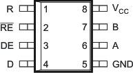
SN65HVD1780 SN65HVD1781 SN65HVD1782 po_lls877.gif

Pin Functions

PIN I/O DESCRIPTION
NAME NUMBER
A 6 Bus input/output Driver output or receiver input (complimentary to B)
B 7 Bus input/output Driver output or receiver input (complimentary to A)
D 4 Digital input Driver data input
DE 3 Digital input Driver enable high
GND 5 Reference potential Local device ground
R 1 Digital output Receive data output
RE 2 Digital input Receiver enable low
VCC 8 Supply 4.5-V to 5.5-V supply