JAJSEH6L March 2002 – January 2018 SN74AUC1G126
UNLESS OTHERWISE NOTED, this document contains PRODUCTION DATA.
- 1 特長
- 2 アプリケーション
- 3 概要
- 4 改訂履歴
- 5 Pin Configuration and Functions
- 6 Specifications
- 7 Typical Characteristics
- 8 Parameter Measurement Information
- 9 Detailed Description
- 10Application and Implementation
- 11Power Supply Recommendations
- 12Layout
- 13デバイスおよびドキュメントのサポート
- 14メカニカル、パッケージ、および注文情報
パッケージ・オプション
デバイスごとのパッケージ図は、PDF版データシートをご参照ください。
メカニカル・データ(パッケージ|ピン)
- DBV|5
- DCK|5
- YZP|5
サーマルパッド・メカニカル・データ
発注情報
8 Parameter Measurement Information
Unless otherwise noted, all input pulses are supplied by generators that have the following characteristics:
- PRR ≤ 10 MHz
- ZO = 50 Ω

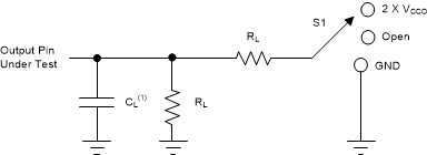
1. CL includes probe and jig capacitance.
Figure 9. Load CircuitTable 1. Loading Conditions for Parameter
| TEST | S1 |
|---|---|
| tPLH (1), tPHL (1) | Open |
| tPLZ (2), tPZL (3) | 2 × VCC |
| tPHZ (2), tPZH (3) | GND |
Table 2. Loading Conditions for VCC
| VCC | CL | RL | VΔ |
|---|---|---|---|
| 0.8 V | 15 pF | 2 kΩ | 0.1 V |
| 1.2 V ± 0.1 V | 15 pF | 2 kΩ | 0.1 V |
| 1.5 V ± 0.1 V | 15 pF | 2 kΩ | 0.1 V |
| 1.8 V ± 0.15 V | 15 pF | 2 kΩ | 0.15 V |
| 2.5 V ± 0.2 V | 15 pF | 2 kΩ | 0.15 V |
| 1.8 V ± 0.15 V | 30 pF | 1 kΩ | 0.15 V |
| 2.5 V ± 0.2 V | 30 pF | 500 kΩ | 0.15 V |
 Figure 10. Voltage Waveforms: Pulse Duration
1. All outputs are measured one at a time, with one transition per measurement.
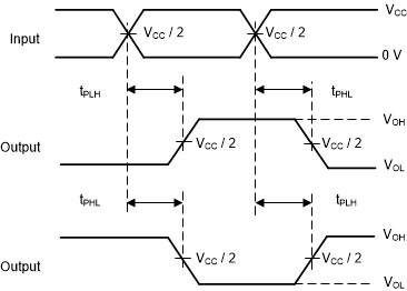
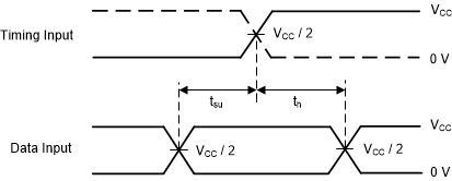
Figure 11. Voltage Waveforms: Propagation Delay Times, Inverting and Noninverting Outputs  Figure 12. Voltage Waveforms: Setup and Hold Times
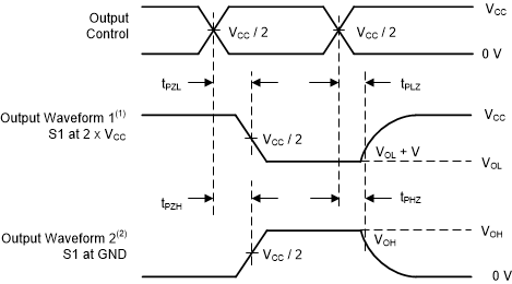
1. Waveform 1 is for an output with internal conditions such as the output is low, except when disabled by the output control.
2. Waveform 2 is for an output with internal conditions such as the output is high, except when disabled by the output control.
3. All outputs are measured one at a time, with one transition per measurement.
Figure 13. Voltage Waveforms: Enable and Disable Times, Low- and High-Level Enabling