SCES626E MARCH 2005 – June 2017 SN74AUC1G19
UNLESS OTHERWISE NOTED, this document contains PRODUCTION DATA.
- 1 Features
- 2 Applications
- 3 Description
- 4 Revision History
- 5 Pin Configuration and Functions
- 6 Specifications
- 7 Parameter Measurement Information
- 8 Detailed Description
- 9 Device and Documentation Support
- 10Mechanical, Packaging, and Orderable Information
パッケージ・オプション
メカニカル・データ(パッケージ|ピン)
サーマルパッド・メカニカル・データ
- DCK|6
発注情報
1 Features
- Latch-Up Performance Exceeds 100 mA Per JESD 78, Class II
- ESD Protection Exceeds JESD 22
- 2000-V Human-Body Model (A114-A)
- 200-V Machine Model (A115-A)
- 1000-V Charged-Device Model (C101)
- Available in the Texas Instruments NanoFree™ Package
- Optimized for 1.8-V Operation and Is 3.6-V I/O Tolerant to Support Mixed-Mode Signal Operation
- Ioff Supports Partial-Power-Down Mode Operation
- Sub-1-V Operable
- ±8-mA Output Drive at 1.8 V VCC
- Maximum tpd of 3 ns at 1.8 V
- Low Power Consumption, 10-µA Maximum ICC
2 Applications
- AV Receiver
- Audio Dock: Portable
- Blu-ray Player and Home Theater
- Embedded PC
- MP3 Player/Recorder (Portable Audio)
- Personal Digital Assistant (PDA)
- Power: Telecom/Server AC/DC Supply: Single Controller: Analog and Digital
- Solid State Drive (SSD): Client and Enterprise
- TV: LCD/Digital and High-Definition (HDTV)
- Tablet: Enterprise
- Video Analytics: Server
- Wireless Headset, Keyboard, and Mouse
3 Description
This 1-of-2 decoder/demultiplexer is operational at 0.8-V to 2.7-V VCC, but is designed specifically for 1.65-V to 1.95-V VCC operation.
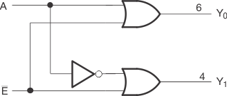
The SN74AUC1G19 is a 1-of-2 decoder/demultiplexer. This device buffers the data on input A and passes it to the outputs Y0 (true) and Y1 (complement) when the enable (E) input signal is low.
NanoFree™ package technology is a major breakthrough in IC packaging concepts, using the die as the package.
This device is fully specified for partial-power-down applications using Ioff. The Ioff circuitry disables the outputs, preventing damaging current backflow through the device when it is powered down.
For more information about AUC Little Logic devices, see Applications of Texas Instruments AUC Sub-1-V Little Logic Devices, SCEA027.
Device Information(1)
| PART NUMBER | PACKAGE | BODY SIZE (NOM) |
|---|---|---|
| SN74AUC1G19DBV | SOT-23 (6) | 2.90 mm × 1.60 mm |
| SN74AUC1G19DCK | SC70 (6) | 2.00 mm × 1.25 mm |
| SN74AUC1G19DRL | SOT-5X3 (6) | 1.60 mm × 1.20 mm |
| SN74AUC1G19YZP | DSBGA (6) | 1.50 mm × 0.90 mm |
- For all available packages, see the orderable addendum at the end of the data sheet.
Logic Diagram (Positive Logic)
