SCES416N December 2002 – January 2017 SN74LVC1G97
PRODUCTION DATA.
- 1 Features
- 2 Applications
- 3 Description
- 4 Revision History
- 5 Pin Configuration and Functions
- 6 Specifications
- 7 Parameter Measurement Information
- 8 Detailed Description
- 9 Application and Implementation
- 10Power Supply Recommendations
- 11Layout
- 12Device and Documentation Support
- 13Mechanical, Packaging, and Orderable Information
パッケージ・オプション
メカニカル・データ(パッケージ|ピン)
サーマルパッド・メカニカル・データ
発注情報
9 Application and Implementation
NOTE
Information in the following applications sections is not part of the TI component specification, and TI does not warrant its accuracy or completeness. TI’s customers are responsible for determining suitability of components for their purposes. Validate and test the design implementation to confirm system functionality.
9.1 Application Information
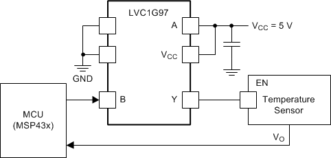
The SN74LVC1G97 device offers flexible configuration for many design applications. This example describes basic power sequencing using the AND gate configuration. Power sequencing is often used in applications that require a processor or other delicate device with specific voltage timing requirements in order to protect the device from malfunctioning.
 Figure 10. Simplified Application
9.2 Typical Application
 Figure 11. Typical Application
9.2.1 Design Requirements
- Recommended input conditions:
- For rise time and fall time specifications, see Δt/Δv in the Recommended Operating Conditions table.
- For specified high and low levels, see VIH and VIL in the Recommended Operating Conditions table.
- Inputs and outputs are overvoltage tolerant and can therefore go as high as 5.5 V at any valid VCC.
- Recommended output conditions:
- Load currents must not exceed ±50 mA.
- Frequency selection criterion:
9.2.2 Detailed Design Procedure
The SN74LVC1G97 device uses CMOS technology and has balanced output drive. Avoid bus contentions that can drive currents that can exceed maximum limits.
The SN74LVC1G97 allows for performing logical Boolean functions with digital signals. Maintain input signals as close as possible to either 0 V or VCC for optimal operation.
9.2.3 Application Curve
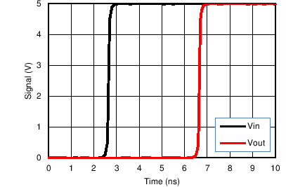
 Figure 12. Simulated Input-to-Output Voltage Response Showing Propagation Delay at VCC = 5 V