SLES270A November 2012 – April 2015 TAS5548
PRODUCTION DATA.
- 1 Features
- 2 Applications
- 3 Description
- 4 Revision History
- 5 Pin Configuration and Functions
-
6 Specifications
- 6.1 Absolute Maximum Ratings
- 6.2 ESD Ratings
- 6.3 Recommended Operating Conditions
- 6.4 Thermal Information
- 6.5 Electrical Characteristics
- 6.6 Dynamic Performance
- 6.7 SRC Performance
- 6.8 Timing I2C Serial Control Port Operation
- 6.9 Reset Timing (RESET)
- 6.10 Power-Down (PDN) Timing
- 6.11 Back-End Error (BKND_ERR)
- 6.12 Mute Timing (MUTE)
- 6.13 Headphone Select (HP_SEL)
- 6.14 Switching Characteristics - Clock Signals
- 6.15 Switching Characteristics - Serial Audio Port
- 6.16 Volume Control
- 6.17 Typical Characteristics
-
7 Detailed Description
- 7.1 Overview
- 7.2 Functional Block Diagram
- 7.3 Feature Description
- 7.4
Device Functional Modes
- 7.4.1 Power Supply
- 7.4.2 Clock, PLL, and Serial Data Interface
- 7.4.3 Serial Audio Interface
- 7.4.4 I 2C Serial-Control Interface
- 7.4.5 Device Control
- 7.4.6 Energy Manager
- 7.4.7 Digital Audio Processor (DAP)
- 7.4.8 Pulse Width Modulation Schemes
- 7.4.9 TAS5548 DAP Architecture Diagrams
- 7.4.10 I 2C Coefficient Number Formats
- 7.4.11 Input Crossbar Mixer
- 7.4.12 Biquad Filters
- 7.4.13 Bass and Treble Controls
- 7.4.14 Volume, Automute, and Mute
- 7.4.15 Loudness Compensation
- 7.4.16 Dynamic Range Control (DRC)
- 7.4.17 THD Manager
- 7.4.18 Downmix Algorithm and I2S Out
- 7.4.19 Stereo Downmixes/(or Fold-Downs)
- 7.4.20 Output Mixer
- 7.4.21 Device Configuration Controls
- 7.4.22 Master Clock and Serial Data Rate Controls
- 7.5 Programming
- 7.6
Register Maps
- 7.6.1 Serial-Control I2C Register Summary
- 7.6.2
Serial-Control Interface Register Definitions
- 7.6.2.1 General Status Register 0 (0x01)
- 7.6.2.2 Error Status Register (0x02)
- 7.6.2.3 System Control Register 1 (0x03)
- 7.6.2.4 System Control Register 2 (0x04)
- 7.6.2.5 Channel Configuration Control Registers (0x05-0x0C)
- 7.6.2.6 Headphone Configuration Control Register (0x0D)
- 7.6.2.7 Serial Data Interface Control Register (0x0E)
- 7.6.2.8 Soft Mute Register (0x0F)
- 7.6.2.9 Energy Manager Status Register (0x10)
- 7.6.2.10 Automute Control Register (0x14)
- 7.6.2.11 Output Automute PWM Threshold and Back-End Reset Period Register (0x15)
- 7.6.2.12 Modulation Index Limit Register (0x16, 0x17, 0x18, 0x19)
- 7.6.2.13 AD Mode - 8 Interchannel Channel Delay and Global Offset Registers (0x1B to 0x23)
- 7.6.2.14 Special Low Z and Mid Z Ramp/Stop Period (0x24)
- 7.6.2.15 PWM and EMO Control Register (0x25)
- 7.6.2.16 Individual Channel Shutdown (0x27)
- 7.6.2.17 Input Mux Registers (0x30, 0x31, 0x32, 0x33)
- 7.6.2.18 PWM Mux Registers (0x34, 0x35, 0x36, 0x37)
- 7.6.2.19 BD Mode and Ternary - 8 Interchannel Channel Delay (0x38 to 0x3F)
- 7.6.2.20 Input Mixer Registers, Channels 1-8 (0x41-0x48)
- 7.6.2.21 Bass Mixer Registers (0x49-0x50)
- 7.6.2.22 Biquad Filter Register (0x51-0x88)
- 7.6.2.23 Bass and Treble Register, Channels 1-8 (0x89-0x90)
- 7.6.2.24 Loudness Registers (0x91-0x95)
- 7.6.2.25 DRC1 Control Register CH1-7 (0x96) - Write
- 7.6.2.26 DRC2 Control Register CH8 (0x97) - Write Register
- 7.6.2.27 DRC1 Data Registers (0x98-0x9C)
- 7.6.2.28 DRC2 Data Registers (0x9D-0xA1)
- 7.6.2.29 DRC Bypass Registers (0xA2-0xA9)
- 7.6.2.30 Output Select and Mix Registers 8x2 (0x-0xAF)
- 7.6.2.31 8×3 Output Mixer Registers (0xB0-0xB1)
- 7.6.2.32 ASRC Registers (0xC3-C5)
- 7.6.2.33 Auto Mute Behavior (0xCC)
- 7.6.2.34 PSVC Volume Biquad Register (0xCF)
- 7.6.2.35 Volume, Treble, and Bass Slew Rates Register (0xD0)
- 7.6.2.36 Volume Registers (0xD1-0xD9)
- 7.6.2.37 Bass Filter Set Register (0xDA)
- 7.6.2.38 Bass Filter Index Register (0xDB)
- 7.6.2.39 Treble Filter Set Register (0xDC)
- 7.6.2.40 Treble Filter Index (0xDD)
- 7.6.2.41 AM Mode Register (0xDE)
- 7.6.2.42 PSVC Range Register (0xDF)
- 7.6.2.43 General Control Register (0xE0)
- 7.6.2.44 96kHz Dolby Downmix Coefficients (0xE3 to 0xE8)
- 7.6.2.45 THD Manager Configuration (0xE9 and 0xEA)
- 7.6.2.46 SDIN5 Input Mixer (0xEC-0xF3)
- 7.6.2.47 192kHZ Process Flow Output Mixer (0xF4-0xF7)
- 7.6.2.48 192kHz Dolby Downmix Coefficients (0xFB and 0xFC)
- 8 Application and Implementation
- 9 Power Supply Recommendations
- 10Layout
- 11Device and Documentation Support
- 12Mechanical, Packaging, and Orderable Information
パッケージ・オプション
メカニカル・データ(パッケージ|ピン)
- DCA|56
サーマルパッド・メカニカル・データ
- DCA|56
発注情報
6 Specifications
6.1 Absolute Maximum Ratings(1)
| MIN | MAX | UNIT | |||
|---|---|---|---|---|---|
| Supply voltage, DVDD1 and DVDD2 | –0.3 | 3.9 | V | ||
| Supply voltage, AVDD and AVDD_PWM | –0.3 | 3.9 | V | ||
| Input voltage | 3.3-V digital input | –0.5 | DVDD + 0.5 | V | |
| 5-V tolerant(2) digital input | –0.5 | 6 | |||
| IIK | Input clamp current (VI < 0 or VI > 1.8 V | ±20 | μA | ||
| IOK | Output clamp current (VO < 0 or VO > 1.8 V) | ±20 | μA | ||
| TSTG | Storage temperature range | –65 | 150 | °C | |
(1) Stresses beyond those listed under Absolute Maximum Ratings may cause permanent damage to the device. These are stress ratings only. Functional operation of the device at these or any other conditions beyond those indicated under Recommended Operating Conditions are not implied. Exposure to absolute-maximum-rated conditions for extended periods may affect device reliability.
(2) 5-V tolerant signals are RESET, PDN, MUTE, HP_SEL, SCLK, LRCLK, MCLK, SDIN1, SDIN2, SDIN3, SDIN4, SDA, and SCL.
6.2 ESD Ratings
| VALUE | UNIT | |||
|---|---|---|---|---|
| V(ESD) | Electrostatic discharge | Human body model (HBM), per ANSI/ESDA/JEDEC JS-001, all pins (1) | ±250 | V |
| Charged device model (CDM), per JEDEC specification JESD22-C101, all pins (2) | ±1000 | V |
(1) JEDEC document JEP155 states that 500-V HBM allows safe manufacturing with a standard ESD control process.
(2) JEDEC document JEP157 states that 250-V CDM allows safe manufacturing with a standard ESD control process.
6.3 Recommended Operating Conditions
over 0°C to 85°C| MIN | NOM | MAX | UNIT | |||
|---|---|---|---|---|---|---|
| Digital supply voltage, DVDD1 and DVDD2 | 3 | 3.3 | 3.6 | V | ||
| Analog supply voltage, AVDD and AVDD_PWM | 3 | 3.3 | 3.6 | V | ||
| VIH | High‐level input voltage | 3.3 V | 2 | V | ||
| 5-V tolerant | 2 | |||||
| 1.8-V LVCMOS (XTL_IN) | 1.26 | |||||
| VIL | Low‐level input voltage | 3.3 V | 0.8 | V | ||
| 5-V tolerant | 0.8 | |||||
| 1.8-V (XTL_IN) | 0.54 | |||||
| TA | Operating ambient-air temperature | 0 | 25 | 85 | °C | |
| TJ | Operating junction temperature | 0 | 105 | °C | ||
6.4 Thermal Information
| THERMAL METRIC(1) | TAS5548 | UNIT | |
|---|---|---|---|
| DCA (HTSSOP) | |||
| 56 PINS | |||
| RθJA | Junction-to-ambient thermal resistance | 26.1 | °C/W |
| RθJCtop | Junction-to-case (top) thermal resistance | 13.0 | |
| RθJB | Junction-to-board thermal resistance | 8.0 | |
| ψJT | Junction-to-top characterization parameter | 0.4 | |
| ψJB | Junction-to-board characterization parameter | 7.9 | |
| RθJCbot | Junction-to-case (bottom) thermal resistance | 0.4 | |
(1) For more information about traditional and new thermal metrics, see the IC Package Thermal Metrics application report, SPRA953.
6.5 Electrical Characteristics
At recommended operating conditions - 25 °C Operating Temp, 3.3V Power Supplies with 48kHz input data unless otherwise specified| PARAMETER | TEST CONDITIONS | MIN | TYP | MAX | UNIT | ||
|---|---|---|---|---|---|---|---|
| VOH | High-level output voltage | 3.3-V TTL and 5-V tolerant | IOH = –4 mA | 2.4 | V | ||
| 1.8-V LVCMOS (XTL_OUT) | IOH = –0.55 mA | 1.44 | |||||
| VOL | Low-level output voltage | 3.3-V TTL and 5-V tolerant | IOL = 4 mA | 0.5 | V | ||
| 1.8-V LVCMOS (XTL_OUT) | IOL = 0.75 mA | 0.5 | |||||
| IOZ | High-impedance output current | 3.3-V TTL | ±20 | μA | |||
| IIL | Low-level input current | 3.3-V TTL | VI = VIL | ±1 | μA | ||
| 1.8-V LVCMOS (XTL_IN) | VI = VIL | ±1 | |||||
| 5-V tolerant(2) | VI = 0 V, DVDD = 3 V | ±1 | |||||
| IIH | High-level input current | 3.3-V TTL | VI = VIH | ±1 | μA | ||
| 1.8-V LVCMOS (XTL_IN) | VI = VIH | ±1 | |||||
| 5-V tolerant(2) | VI = 5.5 V, DVDD = 3 V | ±1 | |||||
| IDD | Input supply current | Digital supply voltage, DVDD | Input fS = 48 kHz | 220 | mA | ||
| Power down | 9 | ||||||
| Analog supply voltage, AVDD | Input fS = 48 kHz | 8 | |||||
| Power down | 8 | ||||||
6.6 Dynamic Performance
At recommended operating conditions at (25°C, 3.3V Power Supplies with 48kHz input data) unless otherwise noted.| PARAMETER | TEST CONDITIONS | MIN | NOM | MAX | UNIT |
|---|---|---|---|---|---|
| Dynamic range | TAS5548 A-weighted (Test Range: 20Hz to 20kHz. fS = 96 kHz). | 105 | dB | ||
| Total harmonic distortion | TAS5548 output (1kHz at -1dBFS) | 0.01% | |||
| Frequency response | 32-kHz to 96-kHz sample rates (Test Range 20Hz - 20kHz) | ±0.1 | dB | ||
| 176.4, 192-kHz sample rates (Test Range 20Hz - 20kHz) | ±0.2 |
6.7 SRC Performance
| ATTRIBUTE | VALUE |
|---|---|
| SRC Latency | 102.53125/FSin + 36.46875/FSout |
| THD+N at 1kHz | |
| Pass Band Ripple (worst case) | ±0.05dB |
| SRC Channel Gain | <1 (slightly lower to compensate for ripple) |
| Stop Band Attenuation | 130dB |
| Pass Band Edge | 0.425 FS-in |
| Stop Band Edge | 0.575 FS-in |
6.8 Timing I2C Serial Control Port Operation
Timing Characteristics for I2C Interface Signals over recommended operating conditions (unless otherwise noted)| STANDARD MODE | FAST MODE | UNIT | ||||
|---|---|---|---|---|---|---|
| MIN | MAX | MIN | MAX | |||
| fSCL | SCL clock frequency | 0 | 100 | 0 | 400 | kHz |
| tHD-STA | Hold time (repeated) START condition. After this period, the first clock pulse is generated. | 4 | 0.6 | μs | ||
| tLOW | LOW period of the SCL clock | 4.7 | 1.3 | μs | ||
| tHIGH | HIGH period of the SCL clock | 4 | 0.6 | μs | ||
| tSU-STA | Setup time for repeated START | 4.7 | 0.6 | μs | ||
| tSU-DAT | Data setup time | 250 | 200 | ns | ||
| tHD-DAT | Data hold time | 0 | 3.45 | 0 | 0.9 | μs |
| tr | Rise time of both SDA and SCL, see Figure 1 | 1000 | 20 + 0.1 Cb | 500 | ns | |
| tf | Fall time of both SDA and SCL, see Figure 1 | 300 | 20 + 0.1 Cb | 300 | ns | |
| tSU-STO | Setup time for STOP condition | 4 | 0.6 | μs | ||
| tBUF | Bus free time between a STOP and START condition | 4.7 | 1.3 | μs | ||
| Cb | Capacitive loads for each bus line | 400 | 400 | pF | ||
| VnL | Noise margin at the LOW level for each connected device (including hysteresis) | 0.1 × VDD | 0.1 × VDD | V | ||
| VnH | Noise margin at the HIGH level for each connected device (including hysteresis) | 0.2 × VDD | 0.2 × VDD | V | ||
6.9 Reset Timing (RESET)
Control signal parameters over recommended operating conditions (unless otherwise noted)| PARAMETER | MIN | TYP | MAX | UNIT | |
|---|---|---|---|---|---|
| tr(DMSTATE) | Time to Non PWM Switching low | 400 | ns | ||
| tw(RESET) | Pulse duration, RESET active, see Figure 3 | 400 | None | ns | |
| tr(I2C_ready) | Time to enable I2C | 5 | ms | ||
6.10 Power-Down (PDN) Timing
Control signal parameters over recommended operating conditions (unless otherwise noted)| PARAMETER | MIN | TYP | MAX | UNIT | |
|---|---|---|---|---|---|
| tp(DMSTATE) | Time to Non PWM Switching low | 650 | μs | ||
| Number of MCLKs preceding the release of PDN, see Figure 4 | 5 | ||||
| tsu | Device startup time | 200 | µs | ||
| Time to audio output | 160 | mS | |||
6.11 Back-End Error (BKND_ERR)
Control signal parameters over recommended operating conditions (unless otherwise noted)| PARAMETER | MIN | TYP | MAX | UNIT | |
|---|---|---|---|---|---|
| tw(ER) | Pulse duration, BKND_ERR active, see Figure 5 | 350 | None | ns | |
| tp(valid_low) | Minimum amount of time that device asserts VALID low. | <100 | μs | ||
| tp(valid_high) | I2C programmable to be between <1mS to 1.2 seconds (to avoid glitching with persistent BKND_ERR) | –25 | 25 | % of interval | |
6.12 Mute Timing (MUTE)
Control signal parameters over recommended operating conditions (unless otherwise noted). See Figure 6| PARAMETER | MIN | TYP | MAX | UNIT | |
|---|---|---|---|---|---|
| td(VOL) | Volume ramp time | Defined by rate setting(1) | ms | ||
Note: No I2C commands during the volume ramp up/down.
6.13 Headphone Select (HP_SEL)
Control signal parameters over recommended operating conditions (unless otherwise noted)| PARAMETER | MIN | TYP | MAX | UNIT | |
|---|---|---|---|---|---|
| tw(HP_SEL) | Pulse duration, HP_SEL active, see Figure 7 | 165 | ms | ||
| td(VOL) | Soft volume update time | Defined by rate setting(1) | ms | ||
| t(SW) | Switchover time | 165 | ms | ||
6.14 Switching Characteristics - Clock Signals
PLL input parameters and external filter components over recommended operating conditions (unless otherwise noted)| PARAMETER | TEST CONDITIONS | MIN | TYP | MAX | UNIT | |
|---|---|---|---|---|---|---|
| External PLL filter capacitors | SMD 0603 X7R | 100 | nF | |||
| External PLL filter capacitors | SMD 0603 X7R | 10 | nF | |||
| External PLL filter resistors | SMD 0603, metal film, 1% | 200 | Ω | |||
| External VR_PWM decoupling C14 | SMD 0603 X7R | 100 | nF | |||
| TAS5548: XTAL Frequency | 12.288 | MHz | ||||
| TAS5548: XTAL Frequency Tolerance at 25°C | ±50 | ppm | ||||
| TAS5548: XTAL Load Capacitance | Follow XTAL Manufacturer specification | |||||
6.15 Switching Characteristics - Serial Audio Port
Serial audio port slave mode over recommended operating conditions (unless otherwise noted)| PARAMETER | TEST CONDITIONS | MIN | TYP | MAX | UNIT | |
|---|---|---|---|---|---|---|
| fSCLKIN | SCLK input frequency | CL = 30 pF | 2.048 | 12.288 | MHz | |
| tsu1 | Setup time, LRCLK to SCLK rising edge | 10 | ns | |||
| th1 | Hold time, LRCLK from SCLK rising edge | 10 | ns | |||
| tsu2 | Setup time, SDIN to SCLK rising edge | 10 | ns | |||
| th2 | Hold time, SDIN from SCLK rising edge | 10 | ns | |||
| LRCLK frequency | 32 | 48 | 192 | kHz | ||
| SCLK rising edges between LRCLK rising edges | 64 | 64 | SCLK edges | |||
| SDOUT delay with respect to SCLK output (load = 30pF), see Figure 8 | 20 | ns | ||||
6.16 Volume Control
Control signal parameters over recommended operating conditions (unless otherwise noted)| PARAMETER | TEST CONDITIONS | MIN | MAX | UNIT |
|---|---|---|---|---|
| Maximum attenuation before mute | Individual volume, master volume, or a combination of both | –127 | dB | |
| Maximum gain | Individual volume, master volume | 18 | dB | |
| Maximum volume before the onset of clipping | 0-dB input, any modulation limit | 0 | dB | |
| PSVC range | PSVC enabled | 12, 18, or 24 | dB | |
| PSVC rate | fS | |||
| PSVC modulation | Single sided | |||
| PSVC quantization | 2048 | Steps | ||
| PSVC PWM modulation limits | PSVC range = 24 dB | 6% (120 : 2048) |
95% (1944 : 2048) |
dB |
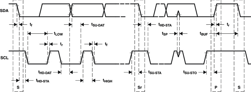 Figure 1. SCL and SDA Timing
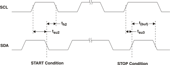 Figure 2. START and STOP Conditions Timing
 Figure 3. Reset Timing
 Figure 4. Power-Down Timing
 Figure 5. Error-Recovery Timing
 Figure 6. Mute Timing
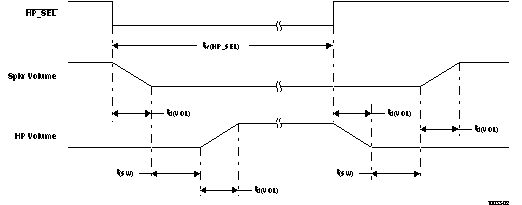 Figure 7. HP_SEL Timing
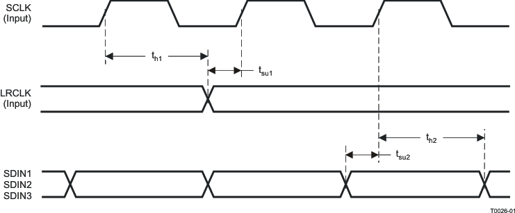 Figure 8. Slave Mode Serial Data Interface Timing
6.17 Typical Characteristics
