SLVS036N September 1981 – January 2015 TL783
PRODUCTION DATA.
- 1 Features
- 2 Applications
- 3 Description
- 4 Simplified Schematic
- 5 Revision History
- 6 Pin Configuration and Functions
- 7 Specifications
- 8 Detailed Description
- 9 Application and Implementation
- 10Power Supply Recommendations
- 11Layout
- 12Device and Documentation Support
- 13Mechanical, Packaging, and Orderable Information
パッケージ・オプション
メカニカル・データ(パッケージ|ピン)
サーマルパッド・メカニカル・データ
- KTT|3
発注情報
8 Detailed Description
8.1 Overview
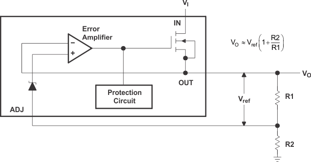
The TL783 device is an adjustable three-terminal high-voltage regulator with an output range of 1.25 V to 125 V and a DMOS output transistor capable of sourcing more than 700 mA. It is designed for use in high-voltage applications where standard bipolar regulators cannot be used. Excellent performance specifications, superior to those of most bipolar regulators, are achieved through circuit design and advanced layout techniques.
As a state-of-the-art regulator, the TL783 device combines standard bipolar circuitry with high-voltage double-diffused MOS transistors on one chip, to yield a device capable of withstanding voltages far higher than standard bipolar integrated circuits. Because of its lack of secondary-breakdown and thermal-runaway characteristics usually associated with bipolar outputs, the TL783 maintains full overload protection while operating at up to 125 V from input to output. Other features of the device include current limiting, safe-operating-area (SOA) protection, and thermal shutdown. Even if ADJ is disconnected inadvertently, the protection circuitry remains functional.
Only two external resistors are required to program the output voltage. An input bypass capacitor is necessary only when the regulator is situated far from the input filter. An output capacitor, although not required, improves transient response and protection from instantaneous output short circuits. Excellent ripple rejection can be achieved without a bypass capacitor at the adjustment terminal.
8.2 Functional Block Diagram
8.3 Feature Description
- Output Adjustable From 1.25 V to 125 V when Used with an External Resistor Divider
- 700-mA Output Current
- Full Short-Circuit, Safe-Operating-Area, and Thermal-Shutdown Protection
- 0.001%/V Typical Input Voltage Regulation
- 0.15% Typical Output Voltage Regulation
- 76-dB Typical Ripple Rejection
8.4 Device Functional Modes
8.4.1 Active Mode
The TL783 acts as a high-voltage adjustable regulator. The device works to keep the voltage at the OUT pin 1.25 V higher than the voltage at the ADJ pin. Therefore, a resistor divider can be used to set the output voltage.