JAJSCX7A February 2017 – December 2017 TLV3201-Q1 , TLV3202-Q1
PRODUCTION DATA.
- 1 特長
- 2 アプリケーション
- 3 概要
- 4 改訂履歴
- 5 Device Comparison Table
- 6 Pin Configuration and Functions
- 7 Specifications
- 8 Detailed Description
- 9 Application and Implementation
- 10Power Supply Recommendations
- 11Layout
- 12デバイスおよびドキュメントのサポート
- 13メカニカル、パッケージ、および注文情報
パッケージ・オプション
メカニカル・データ(パッケージ|ピン)
- DGK|8
サーマルパッド・メカニカル・データ
- DGK|8
発注情報
9.1.1 Comparator Inputs
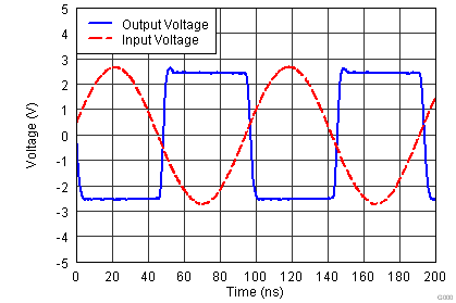
The TLV3201-Q1 and TLV3202-Q1 are rail-to-rail input comparators, with an input common-mode range that exceeds the supply rails by 200 mV for both positive and negative supplies. The devices are specified from 2.7 V to 5.5 V, with room temperature operation from 2.5 V to 5.5 V. The TLV3201-Q1 and TLV3202-Q1 are designed to prevent phase inversion when the input pins exceed the supply voltage. Figure 25 shows the TLV320x-Q1 response when input voltages exceed the supply, resulting in no phase inversion.
 Figure 25. No Phase Inversion: Comparator Response to Input Voltage (Propagation Delay Included)
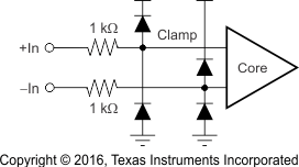
The ESD protection input structure of two back-to-back diodes and 1-kΩ series resistors are used to limit the differential input voltage applied to the precision input of the comparator by clamping input voltages that exceed VCC beyond the specified operating conditions. If potential overvoltage conditions that exceed absolute maximum ratings are present, the addition of external bypass diodes and resistors is recommended, as shown in Figure 26. Large differential voltages greater than the supply voltage must be avoided to prevent damage to the input stage.
 Figure 26. TLV3201-Q1 Equivalent Input structure