SBOS561B March 2012 – December 2016 TLV3201 , TLV3202
UNLESS OTHERWISE NOTED, this document contains PRODUCTION DATA.
- 1 Features
- 2 Applications
- 3 Description
- 4 Revision History
- 5 Device Comparison Table
- 6 Pin Configuration and Functions
- 7 Specifications
- 8 Detailed Description
- 9 Application and Implementation
- 10Power Supply Recommendations
- 11Layout
- 12Device and Documentation Support
- 13Mechanical, Packaging, and Orderable Information
パッケージ・オプション
メカニカル・データ(パッケージ|ピン)
サーマルパッド・メカニカル・データ
- DGK|8
発注情報
9 Application and Implementation
NOTE
Information in the following applications sections is not part of the TI component specification, and TI does not warrant its accuracy or completeness. TI’s customers are responsible for determining suitability of components for their purposes. Customers should validate and test their design implementation to confirm system functionality.
9.1 Application Information
The TLV3201 and TLV3202 are single- and dual-supply (respectively), push-pull comparators featuring 40 ns of propagation delay on only 40 µA of supply current. This combination of fast response time and minimal power consumption make the TLV3201 and TLV3202 excellent comparators for portable, battery-powered applications as well as fast-switching threshold detection such as pulse-width modulation (PWM) output monitors and zero-cross detection.
9.1.1 Comparator Inputs
The TLV3201 and TLV3202 are rail-to-rail input comparators, with an input common-mode range that exceeds the supply rails by 200 mV for both positive and negative supplies. The devices are specified from 2.7 V to 5.5 V, with room temperature operation from 2.5 V to 5.5 V. The TLV3201 and TLV3202 are designed to prevent phase inversion when the input pins exceed the supply voltage. Figure 25 shows the TLV320x response when input voltages exceed the supply, resulting in no phase inversion.
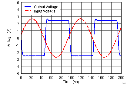 Figure 25. No Phase Inversion: Comparator Response to Input Voltage (Propagation Delay Included)
The electrostatic discharge (ESD) protection input structure of two back-to-back diodes and 1-kΩ series resistors are used to limit the differential input voltage applied to the precision input of the comparator by clamping input voltages that exceed VCC beyond the specified operating conditions. If potential overvoltage conditions that exceed absolute maximum ratings are present, the addition of external bypass diodes and resistors is recommended, as shown in Figure 26. Large differential voltages greater than the supply voltage must be avoided to prevent damage to the input stage.
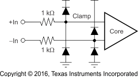 Figure 26. TLV3201 Equivalent Input structure
9.1.2 External Hysteresis
The TLV3201 and TLV3202 have a hysteresis transfer curve (shown in Figure 27) that is a function of three components: VTH, VOS, and VHYST.
- VTH: the actual set voltage or threshold trip voltage
- VOS: the internal offset voltage between VIN+ and VIN–. This voltage is added to VTH to form the actual trip point at which the comparator must respond to change output states.
- VHYST: internal hysteresis (or trip window) that is designed to reduce comparator sensitivity to noise.
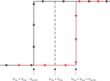 Figure 27. TLV320x Hysteresis Transfer Curve
9.1.2.1 Inverting Comparator with Hysteresis
The inverting comparator with hysteresis requires a three-resistor network that is referenced to the comparator supply voltage (VCC), as shown in Figure 28. When VIN at the inverting input is less than VA, the output voltage is high (for simplicity, assume VO switches as high as VCC). The three network resistors can be represented as R1 || R3 in series with R2. The lower input trip voltage (VA1) is defined by Equation 1.

When VIN is greater than [VA × (VIN > VA)], the output voltage is low, very close to ground. In this case, the three network resistors can be presented as R2 || R3 in series with R1. The upper trip voltage (VA2) is defined by Equation 2.

The total hysteresis provided by the network is defined by Equation 3.

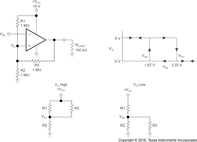 Figure 28. TLV3201 in Inverting Configuration With Hysteresis
9.1.2.2 Noninverting Comparator With Hysteresis
A noninverting comparator with hysteresis requires a two-resistor network, as shown in Figure 29, and a voltage reference (VREF) at the inverting input. When VIN is low, the output is also low. For the output to switch from low to high, VIN must rise up to VIN1. VIN1 is calculated by Equation 4.

When VIN is high, the output is also high. In order for the comparator to switch back to a low state, VIN must equal VREF before VA is again equal to VREF. VIN can be calculated by Equation 5.

The hysteresis of this circuit is the difference between VIN1 and VIN2, as defined by Equation 6.

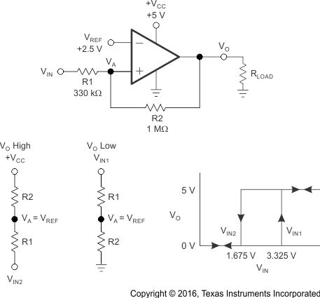 Figure 29. TLV3201 in Noninverting Configuration With Hysteresis
9.1.3 Capacitive Loads
The TLV3201 and TLV3202 feature a push-pull output. When the output switches, there is a direct path between VCC and ground, causing increased output sinking or sourcing current during the transition. Following the transition the output current decreases and supply current returns to 40 µA, thus maintaining low power consumption. Under reasonable capacitive loads, the TLV3201 and TLV3202 maintain specified propagation delay (see Typical Characteristics), but excessive capacitive loading under high switching frequencies may increase supply current, propagation delay, or induce decreased slew rate.
9.2 Typical Applications
9.2.1 TLV3201 Configured as an AC-Coupled Comparator
One of the benefits of AC coupling a single-supply comparator circuit is that it can block dc offsets induced by ground-loop offsets that could potentially produce either a false trip or a common-mode input violation. Figure 30 shows the TLV3201 configured as an ac-coupled comparator.
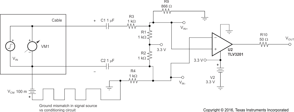 Figure 30. TLV3201 Configured as an AC-Coupled Comparator (Schematic)
9.2.1.1 Design Requirements
Design requirements include:
- Ability to tolerate up to ±100 mV of common-mode signal.
- Trigger only on AC signals (such as zero-cross detection).
9.2.1.2 Detailed Design Procedure
Design analysis:
- AC-coupled, high-pass frequency
- Large capacitors require longer start-up time from device power on
- Use 1-µF capacitor to achieve high-pass frequency of approximately 159 Hz
- For high-pass equivalent, use CIN = 0.5 µF, RIN = 2 kΩ
- Set up input dividers initially for one-half supply (to be in center of acceptable common-mode range).
- Adjust either divider slightly upwards or downwards as desired to establish quiescent output condition.
- Select coupling capacitors based on lowest expected frequency.
9.2.1.3 Application Curve
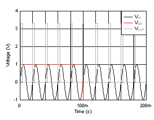 Figure 31. AC-Coupled Comparator Results
9.2.2 TLV3201 and OPA320 Configured as a Fast-Response Output Current Monitor
Figure 32 shows a single-supply current monitor configured as a difference amplifier with a gain of 50. The OPA320 was chosen for this circuit because of its gain bandwidth (20 MHz), which allows higher speed triggering and monitoring of the current across the shunt resistor followed by the fast response of the TLV3201.
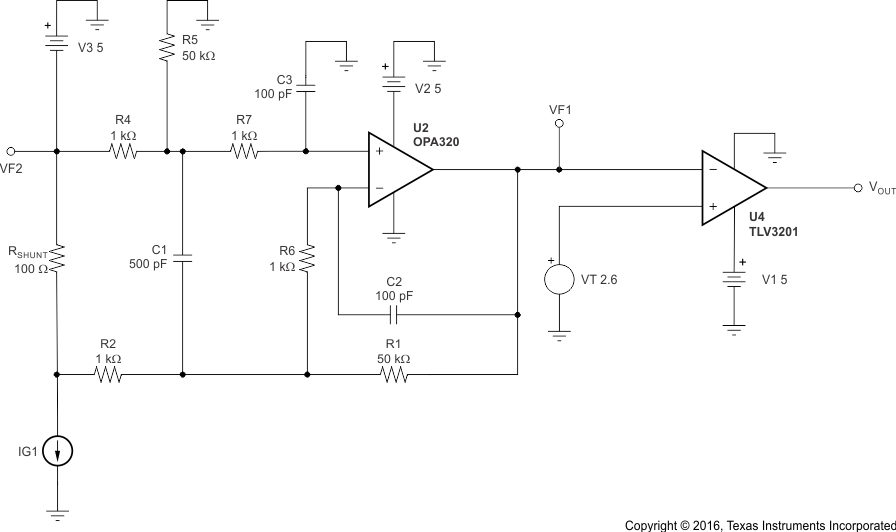 Figure 32. TLV3201 and OPA320 Configured as a Fast-Response Output Current Monitor
9.2.3 TLV3201 and TMP20 Configured as a Precision Analog Temperature Switch
Figure 33 shows the TMP20 and TLV3201 designed as a high-speed temperature switch. The TMP20 is an analog output temperature sensor where output voltage decreases with temperature. The comparator output is tripped when the output reaches a critical trip threshold.
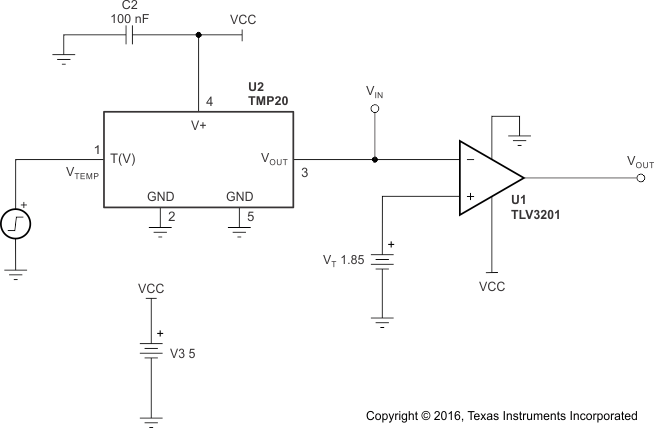 Figure 33. TLV3201 and TMP20 Configured as a Precision Analog Temperature Switch