SBOS561B March   2012  – December 2016 TLV3201 , TLV3202

UNLESS OTHERWISE NOTED, this document contains PRODUCTION DATA.  

  1. Features
  2. Applications
  3. Description
  4. Revision History
  5. Device Comparison Table
  6. Pin Configuration and Functions
  7. Specifications
    1. 7.1 Absolute Maximum Ratings
    2. 7.2 ESD Ratings
    3. 7.3 Recommended Operating Conditions
    4. 7.4 Thermal Information
    5. 7.5 Electrical Characteristics: VCC = 5 V
    6. 7.6 Electrical Characteristics: VCC = 2.7 V
    7. 7.7 Switching Characteristics
    8. 7.8 Typical Characteristics
  8. Detailed Description
    1. 8.1 Overview
    2. 8.2 Functional Block Diagram
    3. 8.3 Feature Description
      1. 8.3.1 Operating Voltage
      2. 8.3.2 Input Overvoltage Protection
    4. 8.4 Device Functional Modes
  9. Application and Implementation
    1. 9.1 Application Information
      1. 9.1.1 Comparator Inputs
      2. 9.1.2 External Hysteresis
        1. 9.1.2.1 Inverting Comparator with Hysteresis
        2. 9.1.2.2 Noninverting Comparator With Hysteresis
      3. 9.1.3 Capacitive Loads
    2. 9.2 Typical Applications
      1. 9.2.1 TLV3201 Configured as an AC-Coupled Comparator
        1. 9.2.1.1 Design Requirements
        2. 9.2.1.2 Detailed Design Procedure
        3. 9.2.1.3 Application Curve
      2. 9.2.2 TLV3201 and OPA320 Configured as a Fast-Response Output Current Monitor
      3. 9.2.3 TLV3201 and TMP20 Configured as a Precision Analog Temperature Switch
  10. 10Power Supply Recommendations
  11. 11Layout
    1. 11.1 Layout Guidelines
    2. 11.2 Layout Example
  12. 12Device and Documentation Support
    1. 12.1 Device Support
      1. 12.1.1 Development Support
        1. 12.1.1.1 TINA-TI™ (Free Software Download)
        2. 12.1.1.2 Universal Op Amp EVM
        3. 12.1.1.3 TI Precision Designs
        4. 12.1.1.4 WEBENCH Filter Designer
    2. 12.2 Documentation Support
      1. 12.2.1 Related Documentation
    3. 12.3 Related Links
    4. 12.4 Receiving Notification of Documentation Updates
    5. 12.5 Community Resource
    6. 12.6 Trademarks
    7. 12.7 Electrostatic Discharge Caution
    8. 12.8 Glossary
  13. 13Mechanical, Packaging, and Orderable Information

パッケージ・オプション

メカニカル・データ(パッケージ|ピン)
サーマルパッド・メカニカル・データ
発注情報

Detailed Description

Overview

The TLV3201 and TLV3202 devices feature 40-ns response time, and include 1.2 mV of internal hysteresis for improved noise immunity with an input common-mode range that extends 0.2 V beyond the power-supply rails.

Functional Block Diagram

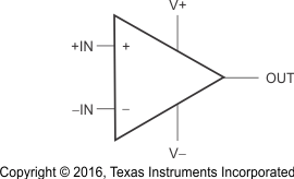
TLV3201 TLV3202 block_diagram_bos561.gif

Feature Description

Operating Voltage

The TLV3201 and TLV3202 comparators are specified for use on a single supply from 2.7 V to 5.5 V (or a dual supply from ±1.35 V to ±2.75 V) over a temperature range of −40°C to 125°C. The device continues to function below this range, but performance is not specified.

Input Overvoltage Protection

The device inputs are protected by electrostatic discharge (ESD) diodes that conduct if the input voltages exceed the power supplies by more than approximately 300 mV. Momentary voltages greater than 300 mV beyond the power supply can be tolerated if the input current is limited to 10 mA. This limiting is easily accomplished with a small input resistor in series with the input to the comparator.

Device Functional Modes

The device is fully functional when powered by rail-to-rail supply voltage greater than 2.7 V. The device is off at any voltages below 2.7 V.