SLAS679A December 2011 – September 2015 TLV320AIC3262
PRODUCTION DATA.
- 1 Features
- 2 Applications
- 3 Description
- 4 Revision History
- 5 Description (continued)
- 6 Device Comparison Table
- 7 Pin Configuration and Functions
-
8 Specifications
- 8.1 Absolute Maximum Ratings
- 8.2 ESD Ratings
- 8.3 Recommended Operating Conditions
- 8.4 Thermal Information
- 8.5 Electrical Characteristics, SAR ADC
- 8.6 Electrical Characteristics, ADC
- 8.7 Electrical Characteristics, Bypass Outputs
- 8.8 Electrical Characteristics, Microphone Interface
- 8.9 Electrical Characteristics, Audio DAC Outputs
- 8.10 Electrical Characteristics, Class-D Outputs
- 8.11 Electrical Characteristics, Miscellaneous
- 8.12 Electrical Characteristics, Logic Levels
- 8.13 I2S/LJF/RJF Timing in Master Mode (see )
- 8.14 I2S/LJF/RJF Timing in Slave Mode (see )
- 8.15 DSP/Mono PCM Timing in Slave Mode (see )
- 8.16 I2C Interface Timing (see )
- 8.17 SPI Interface Timing
- 8.18 Dissipation Ratings
- 8.19 Typical Characteristics
- 9 Parameter Measurement Information
-
10Detailed Description
- 10.1 Overview
- 10.2 Functional Block Diagram
- 10.3
Feature Description
- 10.3.1 Digital Pins
- 10.3.2 Analog Pins
- 10.3.3 Multifunction Pins
- 10.3.4
Analog Audio I/O
- 10.3.4.1 Analog Low Power Bypass
- 10.3.4.2 ADC Bypass Using Mixer Amplifiers
- 10.3.4.3 Headphone Outputs
- 10.3.4.4 Using the Headphone Amplifier
- 10.3.4.5 Ground-Centered Headphone Amplifier Configuration
- 10.3.4.6 Circuit Topology
- 10.3.4.7 Charge Pump Set-Up and Operation
- 10.3.4.8 Output Power Optimization
- 10.3.4.9 Offset Correction and Start-Up
- 10.3.4.10 Ground-Centered Headphone Setup
- 10.3.4.11 Stereo Unipolar Configuration
- 10.3.4.12 Mono Differential DAC to Mono Differential Headphone Output
- 10.3.4.13 Stereo Line Outputs
- 10.3.4.14 Line Out Amplifier Configurations
- 10.3.4.15 Differential Receiver Output
- 10.3.4.16 Stereo Class-D Speaker Outputs
- 10.3.5 ADC / Digital Microphone Interface
- 10.3.6 DAC
- 10.3.7 Powertune
- 10.3.8 Clock Generation and PLL
- 10.3.9 Interfaces
- 10.3.10 Device Special Functions
- 10.3.11 Device Power Consumption
- 10.3.12 Powertune
- 10.3.13 Clock Generation and PLL
- 10.3.14 Interfaces
- 10.3.15 miniDSP
- 10.3.16 Device Special Functions
- 10.4 Device Functional Modes
- 10.5 Register Maps
- 11Application and Implementation
- 12Power Supply Recommendations
- 13Layout
- 14Device and Documentation Support
- 15Mechanical, Packaging, and Orderable Information
11 Application and Implementation
NOTE
Information in the following applications sections is not part of the TI component specification, and TI does not warrant its accuracy or completeness. TI’s customers are responsible for determining suitability of components for their purposes. Customers should validate and test their design implementation to confirm system functionality.
11.1 Application Information
These typical connection diagrams highlight the required external components and system level connections for proper operation of the device in several popular use cases.
Each of these configurations can be realized using the Evaluation Modules (EVMs) for the device. These flexible modules allow full evaluation of the device in all available modes of operation. Additionally, some of the application circuits are available as reference designs and can be found on the TI website. Also see the TLV320AIC3262 product page for information on ordering the EVM. Not all configurations are available as reference designs; however, any design variation can be supported by TI through schematic and layout reviews. Visit www.support.ti.com for additional design assistance. Also, join the audio converters discussion forum at http://e2e.ti.com.
11.2 Typical Application
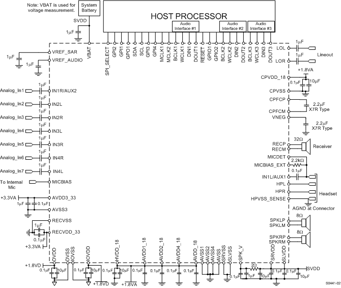
Figure 33 shows a typical circuit configuration for a system utilizing TLV320AIC3262. Note that while this circuit configuration shows all three Audio Serial Interfaces connected to a single Host Processor, it is also quite common for these Audio Serial Interfaces to connect to separate devices (for example Host Processor on Audio Serial Interface number 1, and modems and/or Bluetooth devices on the other audio serial interfaces).
 Figure 33. Typical Circuit Configuration
11.2.1 Design Requirements
This section gives the power-consumption values for various PowerTune modes. All measurements were taken with the PLL turned off and the ADC configured for single-ended input.
Table 14. ADC, Stereo, 48 kHz, Highest Performance, DVDD = IOVDD = 1.8 V, AVDDx_18 = 1.8 V(1)
| DEVICE COMMON MODE SETTING = 0.75 V | DEVICE COMMON MODE SETTING = 0.9 V | UNIT | |||||||
|---|---|---|---|---|---|---|---|---|---|
| PTM_R1 | PTM_R2 | PTM_R3 | PTM_R4 | PTM_R1 | PTM_R2 | PTM_R3 | PTM_R4 | ||
| 0-dB full-scale | X | 375 | 375 | 375 | X | 500 | 500 | 500 | mVRMS |
| Maximum allowed input level w.r.t. 0 dB full scale | X | –12 | 0 | 0 | X | –12 | 0 | 0 | dB full scale |
| Effective SNR w.r.t. maximum allowed input level | X | 78.2 | 91.2 | 91 | X | 79.5 | 93.1 | 93 | dB |
| Power consumption | X | 12.3 | 14.6 | 18.8 | X | 12.3 | 14.6 | 18.8 | mW |
Table 15. Alternative Processing Blocks
| PROCESSING BLOCK | FILTER | ESTIMATED POWER CHANGE (mW) |
|---|---|---|
| PRB_R2 | A | +1.2 |
| PRB_R3 | A | +0.8 |
Table 16. ADC, Stereo, 48 kHz, Lowest Power Consumption(1)
| PTM_R1 CM = 0.75 V AVdd = 1.5 V |
PTM_R3 CM = 0.9 V AVdd = 1.8 V |
UNIT | |
|---|---|---|---|
| 0-dB full-scale | 375 | 500 | mVRMS |
| Maximum allowed input level w.r.t. 0 dB full scale | –2 | 0 | dB full scale |
| Effective SNR w.r.t. maximum allowed input level | 85.9 | 90.8 | dB |
| Power consumption | 5.6 | 9.5 | mW |
Table 17. Alternative Processing Blocks
| PROCESSING BLOCK | FILTER | ESTIMATED POWER CHANGE (mW) |
|---|---|---|
| PRB_R8 | B | +0.4 |
| PRB_R9 | B | +0.2 |
| PRB_R1 | A | +1.2 |
| PRB_R2 | A | +1.8 |
| PRB_R3 | A | +1.6 |
Table 18. DAC, Stereo, 48 kHz, Highest Performance, DVDD = IOVDD = 1.8 V, AVDDx_18 = 1.8 V(1)
| DEVICE COMMON MODE SETTING = 0.75 V | DEVICE COMMON MODE SETTING = 0.9 V | UNIT | ||||||||
|---|---|---|---|---|---|---|---|---|---|---|
| PTM_P1 | PTM_P2 | PTM_P3 | PTM_P4 | PTM_P1 | PTM_P2 | PTM_P3 | PTM_P4 | |||
| 0-dB full-scale | 75 | 225 | 375 | 375 | 100 | 300 | 500 | 500 | mVRMS | |
| Lineout | Effective SNR w.r.t. 0 dB full scale | 89.5 | 96.3 | 99.3 | 99.2 | 91.7 | 98.4 | 101.2 | 101.2 | dB |
| Power consumption | 11.3 | 11.9 | 12.4 | 12.4 | 11.5 | 12.2 | 12.9 | 12.9 | mW | |
Table 19. Alternative Processing Blocks
| PROCESSING BLOCK | FILTER | ESTIMATED POWER CHANGE (mW) |
|---|---|---|
| PRB_P1 | A | –0.1 |
| PRB_P2 | A | +2.6 |
| PRB_P3 | A | +1.1 |
| PRB_P7 | B | –2.8 |
| PRB_P9 | B | –1.7 |
| PRB_P10 | B | +0.6 |
| PRB_P11 | B | –1.2 |
| PRB_P23 | A | –0.1 |
| PRB_P24 | A | +2.8 |
| PRB_P25 | A | +3.6 |
Table 20. DAC, Stereo, 48 kHz, Lowest Power Consumption(1)
| CM = 0.75 V AVdd = 1.5 V PRB_P26 PTM_P1 |
CM = 0.9 V AVdd = 1.8 V PRB_P26 PTM_P1 |
CM = 0.75 V AVdd = 1.5 V PRB_P7 PTM_P4 |
UNIT | ||
|---|---|---|---|---|---|
| 0-dB full-scale | 75 | 100 | 375 | mVRMS | |
| Lineout | Effective SNR w.r.t. 0-dB full-scale | 88.6 | 90.7 | 99.2 | dB |
| Power consumption | 2.7 | 3.3 | 5.2 | mW | |
Table 21. Alternative Processing Blocks
| PROCESSING BLOCK | FILTER | ESTIMATED POWER CHANGE (mW)(1) |
|---|---|---|
| PRB_P1 | A | +3.1 |
| PRB_P2 | A | +4.4 |
| PRB_P3 | A | +3.6 |
| PRB_P7 | B | +1.7 |
| PRB_P9 | B | +2.3 |
| PRB_P10 | B | +3.4 |
| PRB_P11 | B | +2.5 |
| PRB_P23 | A | +3.1 |
| PRB_P24 | A | +4.5 |
| PRB_P25 | A | +4.8 |
For more possible configurations and measurements, please consult the TLV320AIC3262 Applications Reference Guide, SLAU309.
11.2.2 Detailed Design Procedure
For more detailed information see the TLV320AIC3262 Applications Reference Guide, SLAU309.
11.2.2.1 Charge Pump Flying and Holding Capacitor
The TLV320AIC3262 features a built-in charge-pump to generate a negative supply rail, VNEG from CPVDD_18. The negative voltage is used by the headphone amplifier to enable driving the output signal biased around ground potential. For proper operation of the charge pump and headphone amplifier, TI recommends that the flying capacitor connected between CPFCP and CPFCM pins and the holding capacitor connected between VNEG and ground be of X7R type. TI recommends to use 2.2 μF as capacitor value. Failure to use X7R type capacitor can result in degraded performance of charge pump and headphone amplifier.
11.2.2.2 Reference Filtering Capacitor
The TLV320AIC3262 has a built-in bandgap used to generate reference voltages and currents for the device. To achieve high SNR, the reference voltage on VREF_AUDIO should be filtered using a 10-μF capacitor from VREF_AUDIO pin to ground.
11.2.2.3 MICBIAS
TLV320AIC3262 has a built-in bias voltage output for biasing of microphones. No intentional capacitors should be connected directly to the MICBIAS output for filtering
11.2.3 Application Curves
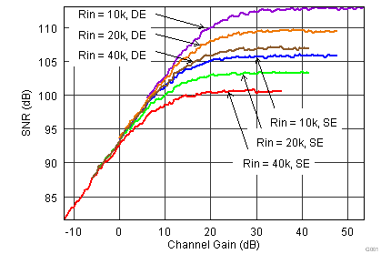
 Figure 34. ADC SNR vs Channel Gain Input-Referred
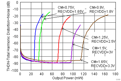
 Figure 35. Total Harmonic Distortion + Noise vs Differential Receiver Output Power 32-Ω Load