JAJSH92A April 2019 – October 2019 TMUX1204
PRODUCTION DATA.
- 1 特長
- 2 アプリケーション
- 3 概要
- 4 改訂履歴
- 5 Pin Configuration and Functions
-
6 Specifications
- 6.1 Absolute Maximum Ratings
- 6.2 ESD Ratings
- 6.3 Recommended Operating Conditions
- 6.4 Thermal Information
- 6.5 Electrical Characteristics (VDD = 5 V ±10 %)
- 6.6 Electrical Characteristics (VDD = 3.3 V ±10 %)
- 6.7 Electrical Characteristics (VDD = 1.8 V ±10 %)
- 6.8 Electrical Characteristics (VDD = 1.2 V ±10 %)
- 6.9 Typical Characteristics
- 7 Parameter Measurement Information
- 8 Detailed Description
- 9 Application and Implementation
- 10Power Supply Recommendations
- 11Layout
- 12デバイスおよびドキュメントのサポート
- 13メカニカル、パッケージ、および注文情報
パッケージ・オプション
メカニカル・データ(パッケージ|ピン)
サーマルパッド・メカニカル・データ
- DQA|10
発注情報
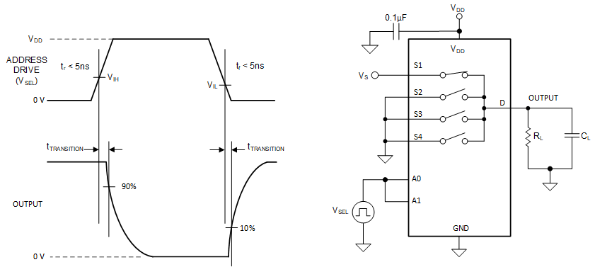
7.4 Transition Time
Transition time is defined as the time taken by the output of the device to rise or fall 10% after the address signal has risen or fallen past the logic threshold. The 10% transition measurement is utilized to provide the timing of the device. System level timing can then account for the time constant added from the load resistance and load capacitance. Figure 10 shows the setup used to measure transition time, denoted by the symbol tTRANSITION.
 Figure 10. Transition-Time Measurement Setup