JAJSH92A April 2019 – October 2019 TMUX1204
PRODUCTION DATA.
- 1 特長
- 2 アプリケーション
- 3 概要
- 4 改訂履歴
- 5 Pin Configuration and Functions
-
6 Specifications
- 6.1 Absolute Maximum Ratings
- 6.2 ESD Ratings
- 6.3 Recommended Operating Conditions
- 6.4 Thermal Information
- 6.5 Electrical Characteristics (VDD = 5 V ±10 %)
- 6.6 Electrical Characteristics (VDD = 3.3 V ±10 %)
- 6.7 Electrical Characteristics (VDD = 1.8 V ±10 %)
- 6.8 Electrical Characteristics (VDD = 1.2 V ±10 %)
- 6.9 Typical Characteristics
- 7 Parameter Measurement Information
- 8 Detailed Description
- 9 Application and Implementation
- 10Power Supply Recommendations
- 11Layout
- 12デバイスおよびドキュメントのサポート
- 13メカニカル、パッケージ、および注文情報
パッケージ・オプション
メカニカル・データ(パッケージ|ピン)
サーマルパッド・メカニカル・データ
- DQA|10
発注情報
11.1.1 Layout Information
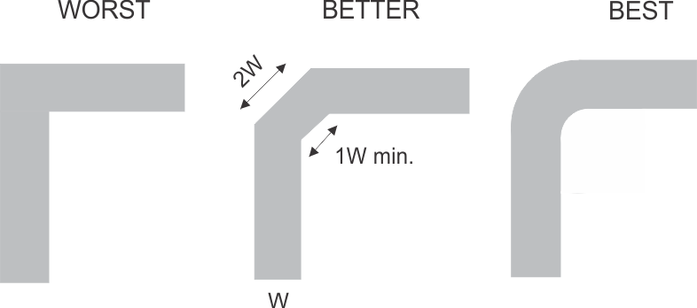
When a PCB trace turns a corner at a 90° angle, a reflection can occur. A reflection occurs primarily because of the change of width of the trace. At the apex of the turn, the trace width increases to 1.414 times the width. This increase upsets the transmission-line characteristics, especially the distributed capacitance and self–inductance of the trace which results in the reflection. Not all PCB traces can be straight and therefore some traces must turn corners.Figure 20 shows progressively better techniques of rounding corners. Only the last example (BEST) maintains constant trace width and minimizes reflections.
 Figure 20. Trace Example
Route high-speed signals using a minimum of vias and corners which reduces signal reflections and impedance changes. When a via must be used, increase the clearance size around it to minimize its capacitance. Each via introduces discontinuities in the signal’s transmission line and increases the chance of picking up interference from the other layers of the board. Be careful when designing test points, through-hole pins are not recommended at high frequencies.
Figure 21 illustrates an example of a PCB layout with the TMUX1204. Some key considerations are:
- Decouple the VDD pin with a 0.1-µF capacitor, placed as close to the pin as possible. Make sure that the capacitor voltage rating is sufficient for the VDD supply.
- Keep the input lines as short as possible.
- Use a solid ground plane to help reduce electromagnetic interference (EMI) noise pickup.
- Do not run sensitive analog traces in parallel with digital traces. Avoid crossing digital and analog traces if possible, and only make perpendicular crossings when necessary.