JAJSGD8B October 2018 – Sept 2019 TMUX1574
PRODUCTION DATA.
- 1 特長
- 2 アプリケーション
- 3 概要
- 4 改訂履歴
- 5 概要 (続き)
- 6 Pin Configuration and Functions
- 7 Specifications
-
8 Parameter Measurement Information
- 8.1 On-Resistance
- 8.2 Off-Leakage Current
- 8.3 On-Leakage Current
- 8.4 IPOFF Leakage Current
- 8.5 Transition Time
- 8.6 tON (EN) and tOFF (EN) Time
- 8.7 tON (VDD) and tOFF (VDD) Time
- 8.8 Break-Before-Make Delay
- 8.9 Propagation Delay
- 8.10 Skew
- 8.11 Charge Injection
- 8.12 Capacitance
- 8.13 Off Isolation
- 8.14 Channel-to-Channel Crosstalk
- 8.15 Bandwidth
- 9 Detailed Description
- 10Application and Implementation
- 11Power Supply Recommendations
- 12Layout
- 13デバイスおよびドキュメントのサポート
- 14メカニカル、パッケージ、および注文情報
パッケージ・オプション
メカニカル・データ(パッケージ|ピン)
サーマルパッド・メカニカル・データ
発注情報
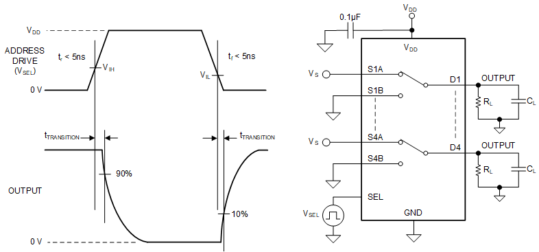
8.5 Transition Time
Transition time is defined as the time taken by the output of the device to rise or fall 10% after the select signal has risen or fallen past the logic threshold. The 10% transition measurement is utilized to provide the timing of the device. The time constant from the load resistance and load capacitance can be added to the transition time to calculate system level timing. Figure 31 shows the setup used to measure transition time, denoted by the symbol tTRANSITION.
 Figure 31. Transition-Time Measurement Setup