SLLSE19F December 2009 – July 2016 TPD12S015
PRODUCTION DATA.
- 1 Features
- 2 Applications
- 3 Description
- 4 Revision History
- 5 Pin Configuration and Functions
-
6 Specifications
- 6.1 Absolute Maximum Ratings
- 6.2 ESD Ratings
- 6.3 Recommended Operating Conditions
- 6.4 Thermal Information
- 6.5 Electrical Characteristics: ICC
- 6.6 Electrical Characteristics: High-Speed ESD Lines: Dx, CLK
- 6.7 Electrical Characteristics: DC-DC Converter
- 6.8 Electrical Characteristics: Passive Components
- 6.9 Electrical Characteristics: Voltage Level Shifter: SCL, SDA Lines (x_A/x_B Ports)
- 6.10 Electrical Characteristics: Voltage Level Shifter: CEC Lines (x_A/x_B Ports)
- 6.11 Electrical Characteristics: Voltage Level Shifter: HPD Line (x_A/x_B Ports)
- 6.12 Electrical Characteristics: LS_OE, CT_CP_HPD
- 6.13 Electrical Characteristics: I/O Capacitance
- 6.14 Switching Characteristics
- 6.15 Switching Characteristics: Voltage Level Shifter: SCL, SDA Lines (x_A & x_B ports); VCCA = 1.2 V
- 6.16 Switching Characteristics: Voltage Level Shifter: CEC Line (x_A & x_B ports); VCCA = 1.2 V
- 6.17 Switching Characteristics: Voltage Level Shifter: HPD Line (x_A & x_B ports); VCCA = 1.2 V
- 6.18 Switching Characteristics: Voltage Level Shifter: SCL, SDA Lines (x_A & x_B ports); VCCA = 1.5 V
- 6.19 Switching Characteristics: Voltage Level Shifter: CEC Line (x_A & x_B ports); VCCA = 1.5 V
- 6.20 Switching Characteristics: Voltage Level Shifter: HPD Line (x_A & x_B ports); VCCA = 1.5 V
- 6.21 Switching Characteristics: Voltage Level Shifter: SCL, SDA Lines (x_A & x_B ports); VCCA = 1.8 V
- 6.22 Switching Characteristics: Voltage Level Shifter: CEC Line (x_A & x_B ports); VCCA = 1.8 V
- 6.23 Switching Characteristics: Voltage Level Shifter: HPD Line (x_A & x_B ports); VCCA = 1.8 V
- 6.24 Switching Characteristics: Voltage Level Shifter: SCL, SDA Lines (x_A & x_B ports); VCCA = 2.5 V
- 6.25 Switching Characteristics: Voltage Level Shifter: CEC Line (x_A & x_B ports); VCCA = 2.5 V
- 6.26 Switching Characteristics: Voltage Level Shifter: HPD Line (x_A & x_B ports); VCCA = 2.5 V
- 6.27 Switching Characteristics: Voltage Level Shifter: SCL, SDA Lines (x_A & x_B ports); VCCA = 3.3 V
- 6.28 Switching Characteristics: Voltage Level Shifter: CEC Line (x_A & x_B ports); VCCA = 3.3 V
- 6.29 Switching Characteristics: Voltage Level Shifter: HPD Line (x_A & x_B ports); VCCA = 3.3 V
- 6.30 Typical Characteristics
- 7 Parameter Measurement Information
- 8 Detailed Description
- 9 Application and Implementation
- 10Power Supply Recommendations
- 11Layout
- 12Device and Documentation Support
- 13Mechanical, Packaging, and Orderable Information
11 Layout
11.1 Layout Guidelines
For proper operation, follow these layout and design guidelines:
- Place the TPD12S015 as close to the connector as possible. This allows it to remove the energy associated with ESD strike before it reaches the internal circuitry of the system board.
- Place power line capacitors and inductors close to the pins with wide traces to allow enough current to flow through with less trace parasitics.
- Ensure that there is enough metallization for the GND pad. A sufficient current path enables safe discharge of all the energy associated with the ESD strike.
- The critical routing paths for HDMI interface are the high-speed TMDS lines. Make sure to match the lengths of the differential pair. Maintain constant trace width after to avoid impedance mismatches in the transmission lines. Maximize differential pair-to-pair spacing when possible.
For more layout information, see TPD12S015 PCB Layout Guidelines.
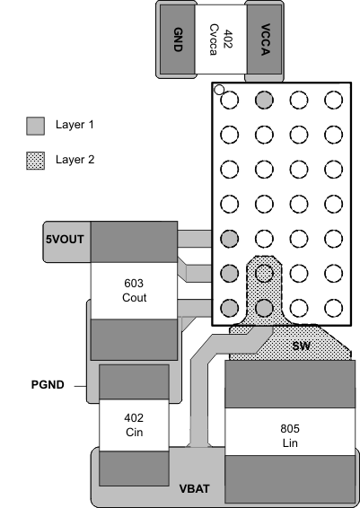
11.2 Layout Example
 Figure 25. Board Layout (DC-DC Components) (Top View)
List of components:
- LIN = MURATA LQM21PN1R0MC0 or LIN = Toko MDT2010-CN1R0
- CIN = MURATA GRM188R60J225ME19 (2.2 µF, 6.3 V, 0603, X5R) or MURATA GRM188R60J475ME19 (4.7 µF, 6.3 V, 0603, X5R)
- COUT = MURATA GRM188R60J475ME19 (4.7 µF, 6.3 V, 0603, X5R)
- CVCCA = MURATA GRM155R60J104MA01 (0.1 µF, 6.3 V, 0402, X5R)