SLLSE96F September 2011 – October 2015 TPD12S016
PRODUCTION DATA.
- 1 Features
- 2 Applications
- 3 Description
- 4 Revision History
- 5 Pin Configuration and Functions
- 6 Specifications
-
7 Detailed Description
- 7.1 Overview
- 7.2 Functional Block Diagram
- 7.3
Feature Description
- 7.3.1 Conforms to HDMI Compliance Tests Without any External Components
- 7.3.2 IEC 61000-4-2 ESD Protection
- 7.3.3 Supports HDMI 1.4 Data Rate
- 7.3.4 Matches Class D and Class C Pin Mapping
- 7.3.5 8-Channel ESD Lines for Four Differential Pairs with Ultra-low Differential Capacitance Matching (0.05 pF)
- 7.3.6 On-Chip Load Switch With 55-mA Current Limit Feature at the HDMI 5V_OUT Pin
- 7.3.7 Auto-direction Sensing I2C Level Shifter With One-Shot Circuit to Drive a Long HDMI Cable (750-pF Load)
- 7.3.8 Back-Drive Protection on HDMI Connector Side Ports
- 7.3.9 Integrated Pullup and Pulldown Resistors per HDMI Specification
- 7.3.10 Space Saving 24-Pin RKT Package and 24-TSSOP Package
- 7.3.11 DDC/CEC LEVEL SHIFT Circuit Operation
- 7.3.12 DDC/CEC Level Shifter Operational Notes For VCCA = 1.8 V
- 7.3.13 Rise-Time Accelerators
- 7.3.14 Noise Considerations
- 7.3.15 Resistor Pullup Value Selection
- 7.4 Device Functional Modes
- 8 Application and Implementation
- 9 Power Supply Recommendations
- 10Layout
- 11Device and Documentation Support
- 12Mechanical, Packaging, and Orderable Information
パッケージ・オプション
デバイスごとのパッケージ図は、PDF版データシートをご参照ください。
メカニカル・データ(パッケージ|ピン)
- RKT|24
- PW|24
サーマルパッド・メカニカル・データ
- RKT|24
発注情報
1 Features
- Conforms to HDMI Compliance Tests without any External Components
- IEC 61000-4-2 ESD Protection
- ±8-kV Contact Discharge
- Supports HDMI 1.4 Data Rate
- Matches Class D and Class C Pin Mapping
- 8-Channel ESD Protection for Four Differential Pairs With Ultra-Low Differential Capacitance Matching (0.05 pF)
- On-Chip Load Switch With 55-mA Current Limit at the HDMI 5V_OUT Pin
- Auto-direction Sensing I2C Level Shifter with One-shot Circuit to Drive a Long HDMI Cable (750-pF Load)
- Back-drive Protection on HDMI Connector Side Ports
- Integrated Pullup and Pulldown Resistors per HDMI Specification
- Space Saving 24-Pin RKT Package and 24-TSSOP Package
2 Applications
- Cell Phones
- eBook
- Portable Media Players
- Set-top Box
3 Description
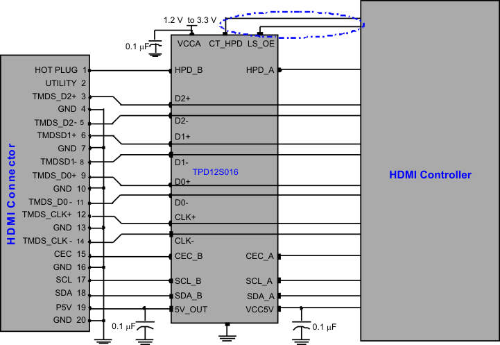
The TPD12S016 is a single-chip High Definition Multimedia Interface (HDMI) device with auto-direction sensing I2C voltage level shift buffers, a load switch, and integrated low capacitance high-speed electrostatic discharge (ESD) transient voltage suppression (TVS) protection diodes. A 55-mA current limited 5-V output (5V_OUT) sources the HDMI power line. The control of 5V_OUT and the hot plug detect (HPD) circuitry is independent of the LS_OE control signal, and is controlled by the CT_HPD pin, which enables the detection scheme (5V_OUT and HPD) to be active before enabling the HDMI link. The SDA, SCL, and CEC lines pull up to VCCA on the A side. On the B side, the CEC_B pin pulls up to an internal 3.3-V supply rail, SCL_B and SDA_B each pull up to the 5-V rail (5V_OUT). The SCL and SDA pins meet the I2C specification and drive up to 750 pF capacitive loads, exceeding the HDMI 1.4 specifications. The HPD_B port has a glitch filter to avoid false detection due to plug bouncing during the HDMI connector insertion. TPD12S016 offers reverse current blocking at the 5V_OUT pin. SCL_B, SDA_B, CEC_B pins also feature reverse-current blocking when the system is powered off.
Device Information(1)
| PART NUMBER | PACKAGE | BODY SIZE (NOM) |
|---|---|---|
| TPD12S016 | QFN (24) | 4.00 mm × 2.00 mm |
| TSSOP (24) | 7.80 mm × 6.40 mm |
- For all available packages, see the orderable addendum at the end of the data sheet.
Simplified Schematic
