SLVSBC5D March 2012 – October 2015 TPD13S523
PRODUCTION DATA.
- 1 Features
- 2 Applications
- 3 Description
- 4 Revision History
- 5 Pin Configuration and Functions
- 6 Specifications
-
7 Detailed Description
- 7.1 Overview
- 7.2 Functional Block Diagram
- 7.3
Feature Description
- 7.3.1 IEC 61000-4-2 Protection
- 7.3.2 Single-Chip ESD Solution
- 7.3.3 On-Chip 5-V Load Switch
- 7.3.4 Supports UTILITY Line Protection
- 7.3.5 < 0.05-pF Differential Capacitance Between TMDS Pairs
- 7.3.6 Industry Standard Package and Space-Saving Package
- 7.3.7 Supports Data Rates in Excess of 3.4 Gbps
- 7.3.8 RDYN = 0.5 Ω
- 7.3.9 Commercial Temperature Range
- 7.4 Device Functional Modes
- 8 Application and Implementation
- 9 Power Supply Recommendations
- 10Layout
- 11Device and Documentation Support
- 12Mechanical, Packaging, and Orderable Information
パッケージ・オプション
メカニカル・データ(パッケージ|ピン)
サーマルパッド・メカニカル・データ
発注情報
5 Pin Configuration and Functions
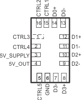
RSV Package
16-Pin UQFN
Top View

All the CTRLx pins have the same ESD circuit and are interchangeable.
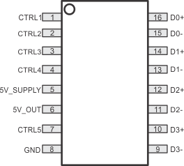
PW Package
16-Pin TSSOP
Top View

All the CTRLx pins have the same ESD circuit and are interchangeable.
Pin Functions
| PIN | I/O | DESCRIPTION | ||
|---|---|---|---|---|
| NAME | UQFN | TSSOP | ||
| CTRL1 | 15 | 1 | I/O | ESD Clamp for Control Lines: provides ESD protection to HDMI control lines: CEC, SCL, SDA, HPD, and UTILITY. All the control pins have the same ESD circuit and are interchangeable.(1) |
| CTRL2 | 16 | 2 | I/O | ESD Clamp for Control Lines: provides ESD protection to HDMI control lines: CEC, SCL, SDA, HPD, and UTILITY. All the control pins have the same ESD circuit and are interchangeable.(1) |
| CTRL3 | 1 | 3 | I/O | ESD Clamp for Control Lines: provides ESD protection to HDMI control lines: CEC, SCL, SDA, HPD, and UTILITY. All the control pins have the same ESD circuit and are interchangeable.(1) |
| CTRL4 | 2 | 4 | I/O | ESD Clamp for Control Lines: provides ESD protection to HDMI control lines: CEC, SCL, SDA, HPD, and UTILITY. All the control pins have the same ESD circuit and are interchangeable.(1) |
| CTRL5 | 5 | 7 | I/O | ESD Clamp for Control Lines: provides ESD protection to HDMI control lines: CEC, SCL, SDA, HPD, and UTILITY. All the control pins have the same ESD circuit and are interchangeable.(1) |
| 5V_SUPPLY | 3 | 5 | I | Supply Pin for HDMI 5V_OUT 5 V, connects to internal VCC plane on the PCB board; connect a 0.1 to 1-µF capacitor shunt to ground. |
| 5V_OUT | 4 | 6 | O | Current Limited HDMI 5V_OUT: connect to HDMI 5V_OUT; offers IEC61000-4-2 ESD protection; connect a 0.1 to 1-µF capacitor shunt to ground. |
| GND | 6 | 8 | G | Ground |
| D0+ | 14 | 16 | I/O | High-speed ESD Clamp: provides ESD protection for TMDS lines.(1) |
| D0– | 13 | 15 | I/O | High-speed ESD Clamp: provides ESD protection for TMDS lines.(1) |
| D1+ | 12 | 14 | I/O | High-speed ESD Clamp: provides ESD protection for TMDS lines.(1) |
| D1– | 11 | 13 | I/O | High-speed ESD Clamp: provides ESD protection for TMDS lines.(1) |
| D2+ | 10 | 12 | I/O | High-speed ESD Clamp: provides ESD protection for TMDS lines.(1) |
| D2– | 9 | 11 | I/O | High-speed ESD Clamp: provides ESD protection for TMDS lines.(1) |
| D3+ | 8 | 10 | I/O | High-speed ESD Clamp: provides ESD protection for TMDS lines.(1) |
| D3– | 7 | 9 | I/O | High-speed ESD Clamp: provides ESD protection for TMDS lines.(1) |
(1) Connector pins are Dx+, Dx–, CTRLx, and 5V_OUT