SLLSEK0A December 2014 – February 2015 TPD6F002-Q1
PRODUCTION DATA.
- 1 Features
- 2 Applications
- 3 Description
- 4 Simplified Schematic
- 5 Revision History
- 6 Pin Configuration and Functions
- 7 Specifications
- 8 Detailed Description
- 9 Application and Implementation
- 10Power Supply Recommendations
- 11Layout
- 12Device and Documentation Support
- 13Mechanical, Packaging, and Orderable Information
パッケージ・オプション
メカニカル・データ(パッケージ|ピン)
- DSV|12
サーマルパッド・メカニカル・データ
- DSV|12
発注情報
9 Application and Implementation
NOTE
Information in the following applications sections is not part of the TI component specification, and TI does not warrant its accuracy or completeness. TI’s customers are responsible for determining suitability of components for their purposes. Customers should validate and test their design implementation to confirm system functionality.
9.1 Application Information
The TPD6F002-Q1 is a highly integrated device that provides a six channel EMI filter and a TVS based ESD protection diode array. The low-pass filter array suppresses EMI/RFI emissions for data ports subject to electromagnetic interference. The TVS diode array is rated to dissipate ESD strikes above the maximum level specified in the IEC 61000-4-2 international standard. The high level of integration, combined with its small easy-to-route DSV package, allows this device to provide great circuit protection for LCD displays, memory interfaces, GPIO lines, and FPD-Link.
9.2 Typical Application
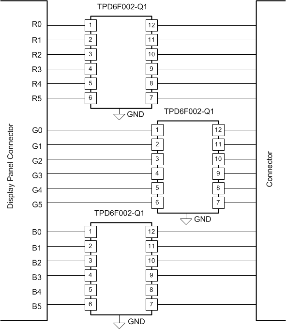 Figure 7. Display Panel Schematic
9.2.1 Design Requirements
For this design example, three TPD6F002-Q1 devices are being used in an 18-bit display panel application. This will provide a complete ESD and EMI protection solution for the display connector.
Given the display panel application, the following parameters are known.
| DESIGN PARAMETER | VALUE |
|---|---|
| Signal range on all pins except GND | 0 V to 5 V |
| Operating Frequency | 50 MHz |
9.2.2 Detailed Design Procedure
To begin the design process, some design parameters must be decided; the designer needs to know the following:
- Signal range of all the protected lines
- Operating frequency
- Crosstalk response
9.2.2.1 Signal Range on All Protected Lines
The TPD6F002-Q1 has 6 identical protection channels for signal lines. All I/O pins will support a signal range from 0 to 5.5 V.
9.2.2.2 Operating Frequency
The TPD6F002-Q1 has a 100 MHz –3 dB bandwidth, which supports the operating frequency for this display.
9.2.2.3 Crosstalk Response
The TPD6F002-Q1 has a –47 dB near-side crosstalk attenuation at 100 MHz, sufficient for this display.
9.2.3 Application Curves
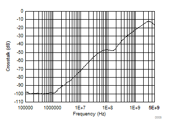 Figure 8. Near-Side Crosstalk