SLDS182A August 2010 – July 2015 TPIC7218-Q1
PRODUCTION DATA.
- 1 Device Overview
- 2 Revision History
- 3 Pin Configuration and Functions
-
4 Specifications
- 4.1 Absolute Maximum Ratings
- 4.2 ESD Ratings
- 4.3 Recommended Operating Conditions
- 4.4 Thermal Information
- 4.5 Input Port Electrical Characteristics
- 4.6 PWM Low-Side Driver Electrical Characteristics
- 4.7 Digital Low-Side Driver Electrical Characteristics
- 4.8 High-Side Driver Electrical Characteristics
- 4.9 K-Line Electrical Characteristics
- 4.10 Warning Lamp Electrical Characteristics
- 4.11 Power Supply Electrical Characteristics
- 4.12 SPI Electrical Characteristics
- 4.13 WL_LS Low-Side Switch Output Characteristics
- 4.14 Wheel-Speed High-Side Driver Characteristics
- 4.15 Wheel-Speed Low-Side Driver Characteristics
- 4.16 Wheel-Speed Output Characteristics
- 4.17 RST Output Characteristics
- 4.18 SPI Timing Electrical Characteristics
- 4.19 Power Supply Switching Characteristics
- 4.20 Wheel-Speed Counter Switching Characteristics
- 4.21 HS Driver Switching Characteristics
- 4.22 Digital Low-Side Driver Switching Characteristics
- 4.23 PWM Low-Side Driver Switching Characteristics
- 4.24 K-Line Switching Characteristics
- 4.25 Warning Lamp Switching Characteristics
- 4.26 Watchdog Switching Characteristics
- 4.27 Wheel Speed Interface Switching Characteristics
- 4.28 Wheel-Speed High-Side Driver Switching Characteristics
- 4.29 Wheel-Speed Output Switching Characteristics
- 4.30 Typical Characteristics
-
5 Detailed Description
- 5.1 Overview
- 5.2 Functional Block Diagram
- 5.3
Feature Description
- 5.3.1 Ground Connections
- 5.3.2 Charge Pump
- 5.3.3 Reference Current Generator
- 5.3.4 Wheel-Speed Reference, VREF
- 5.3.5 Faults Common To Most Functional Blocks
- 5.3.6 PWM Low-Side Drivers
- 5.3.7 Digital Low-Side Drivers
- 5.3.8 High-Side Drivers
- 5.3.9 Wheel-Speed Sensing
- 5.3.10 K-Line
- 5.3.11 Warning Lamp Drivers
- 5.3.12 Watchdog Operation
- 5.4 Device Functional Modes
- 5.5 Programming
- 5.6 Register Maps
- 6 Application and Implementation
- 7 Power Supply Recommendations
-
8 Layout
- 8.1
Layout Guidelines
- 8.1.1 Local Grounding Configuration
- 8.1.2 Board Level Grounding Configuration, TPIC7218-Q1 to System Connector
- 8.1.3 VCC3 Bypass Capacitor
- 8.1.4 VDD Bypass Capacitor
- 8.1.5 VBAT and CHP Capacitors
- 8.1.6 Multiple Plane Layer Assignments
- 8.1.7 Duplicate Pad Under TPIC7218-Q1 on All Non-Ground Plane Inner Layers
- 8.1.8 Flooding
- 8.2 Layout Example
- 8.1
Layout Guidelines
- 9 Device and Documentation Support
- 10Mechanical, Packaging, and Orderable Information
パッケージ・オプション
メカニカル・データ(パッケージ|ピン)
- PFP|80
サーマルパッド・メカニカル・データ
- PFP|80
発注情報
1 Device Overview
1.1 Features
- Qualified for Automotive Applications
- AEC-Q100 Qualified with the Following Results:
- Device Temperature Grade 1: –40°C to 125°C Ambient Operating Temperature Range
- Device HBM ESD Classification Level 2
- Device CDM ESD Classification Level C4
- PWM Low-Side Drivers
- 4 PWM Low-Side Driver Outputs
- Current Limitation
- Thermal Protection: TJ = 185°C (Minimum)
- Open-Load Detection
- Energy Capability: 30 mJ at TJ = 150°C
- Clamp Voltage: 40 V
- Low RDSon: 0.3 Ω (Maximum) at TJ = 150°C
- Digital Low-Side Drivers
- 4 Digital Low-Side Driver Outputs
- Current Limitation
- Thermal Protection: TJ = 185°C (Minimum)
- Open-Load Detection
- Energy Capability: 50 mJ at TJ = 150°C
- Clamp Voltage: 40 V
- Low RDSon: 0.2 Ω (Maximum) at TJ = 150°C
- Dual High-Side Power Drivers
- Direct Input Control
- PWM Capability
- Load Dump (overvoltage) Detection
- Programmable overcurrent detection
- Load Leakage Detection
- Programmable short-circuit Protection
- Fault detection over SPI
- Wheel-Speed Sensor Interface
- Compatible with Intelligent and Active Wheel-Speed Sensors
- 4 High-Side Switches With Short-Circuit Protection
- 4 Low-Side Switches With Short-Circuit Protection
- 2 High Voltage Low-Side Output Drivers
- 4 Digital Outputs to Indicate the Speed
- Integrated Data Decoder for Intelligent Wheel-Speed Sensors
- Open-Drain Warning Lamp Drivers
- 2 High Voltage Drivers
- Thermal Protection With Hysteresis
- Current Limitation
- TJ = 185°C (Minimum)
- RDSon: 4 Ω at TJ = 150°C
- Clamp Voltage: 40 V
- Other Features
- K-LINE Transceiver
- 3.3-V or 5-V Compatible Digital IO
- Internal 3.3-V Regulator
- Internal Charge Pump
- 1 Low-Voltage Open-Drain Warning Lamp Driver
- Full Duplex SPI Interface
- Watchdog Input With Open-Drain Fault Reporting for Safety
- Pb-Free ASIC
- Compliant With CISPR 25 NB Class 5 for Conducted and Radiated Emissions
1.2 Applications
- Anti-lock Braking Systems (ABS)
- Electronic Stability Control Systems (ESC)
1.3 Description
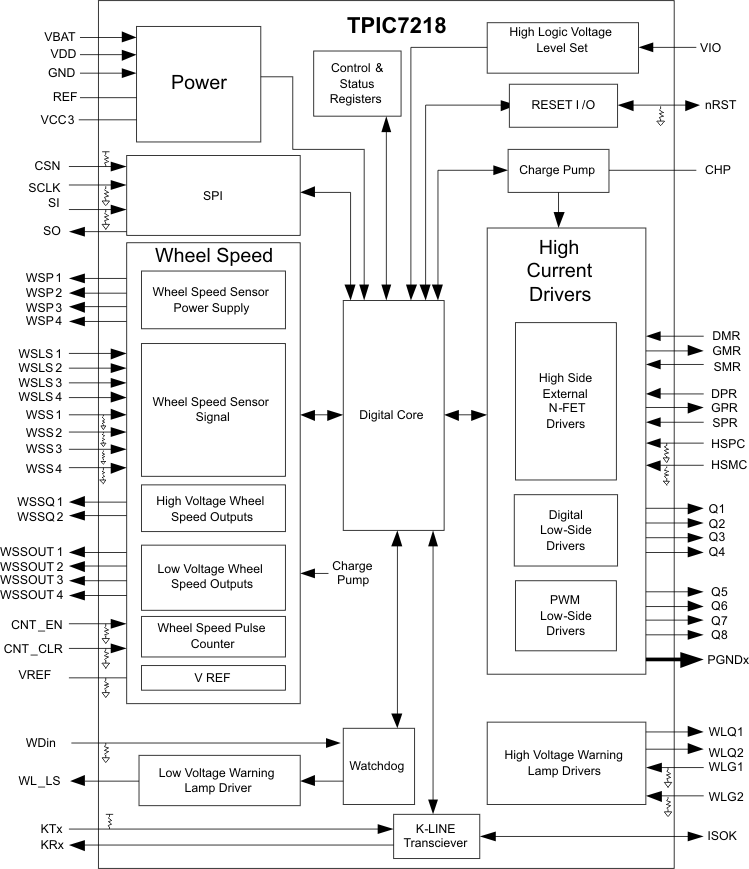
The TPIC7218-Q1 device integrates in single package several functions needed in ABS and ESC electronic control units (ECU). This integration coupled with the minimization of the external components saves valuable ECU board space.
The TPIC7218-Q1 device is an antilock braking controller capable of directly driving eight solenoid valves with internal high-current low-side drivers. Low-side drivers configured for digital control do not require external voltage clamps. The TPIC7218-Q1 device has gate drive capability for two high-side N-Channel MOSFETs that can be used to drive a pump motor and power to all solenoids. The TPIC7218-Q1 device provides a fault-tolerant interface for both Intelligent and Active wheel-speed sensors to an external microprocessor. The TPIC7218-Q1 device can be used with either 3.3- or 5-V microprocessors and uses a standard SPI (Serial-Peripheral Interface).
The TPIC7218-Q1 device has two internal open-drain warning lamp drivers that can be pulled up to battery voltage, as well as one low-voltage driver. An internal state machine monitors a watchdog input and reports faults on a warning-lamp pin and SPI register. A K-Line transceiver is also included. A multitude of safety and fault monitoring functionality supervise both system and TPIC7218-Q1 circuits. Faults must be polled and reset over SPI. The TPIC7218-Q1 device is designed for use in harsh automotive environments, capable of withstanding high operating temperatures and electrically noisy signals and power. Short-to-ground, short-to-battery, and open-load conditions are tolerated and monitored. The TPIC7218-Q1 device also exhibits outstanding Electro-Magnetic Compatibility (EMC) performance.
Device Information(1)
| PART NUMBER | PACKAGE | BODY SIZE (NOM) |
|---|---|---|
| TPIC7218-Q1 | HTQFP (80) | 12.00 mm × 12.00 mm |
1.4 Functional Block Diagram
 Figure 1-1 Functional Block Diagram