SLVSD04 April   2015 TPS22860

PRODUCTION DATA.  

  1. Features
  2. Applications
  3. Description
    1. 3.1 Common Application Schematic
  4. Revision History
  5. Pin Configuration and Functions
  6. Specifications
    1. 6.1 Absolute Maximum Ratings
    2. 6.2 ESD Ratings
    3. 6.3 Recommended Operating Conditions
    4. 6.4 Thermal Information
    5. 6.5 Electrical Characteristics
    6. 6.6 Switching Characteristics
    7. 6.7 Typical Characteristics
  7. Detailed Description
    1. 7.1 Overview
    2. 7.2 Functional Block Diagram
    3. 7.3 Feature Description
      1. 7.3.1 ON/OFF Control
      2. 7.3.2 Pass Transistor
    4. 7.4 Device Functional Modes
  8. Application and Implementation
    1. 8.1 Application Information
    2. 8.2 Typical Application
      1. 8.2.1 Design Requirements
      2. 8.2.2 Detailed Design Procedure
        1. 8.2.2.1 Inrush Current
        2. 8.2.2.2 ON/OFF Interface
      3. 8.2.3 Application Curves
  9. Power Supply Recommendations
  10. 10Layout
    1. 10.1 Layout Guidelines
    2. 10.2 Thermal Reliability
    3. 10.3 Improving Package Thermal Performance
    4. 10.4 Layout Example
    5. 10.5 Trademarks
    6. 10.6 Electrostatic Discharge Caution
    7. 10.7 Glossary
  11. 11Mechanical, Packaging, and Orderable Information

パッケージ・オプション

メカニカル・データ(パッケージ|ピン)
サーマルパッド・メカニカル・データ
発注情報

7 Detailed Description

7.1 Overview

The TPS22860 is a small, ultra-low leakage current, single channel bi-driectional load switch. The device requires a VBIAS voltage and can operate over an input voltage range of 0 V to VBIAS. It can support a maximum continuous current of 200 mA. The switch is controlled by an on/off input (ON), which is capable of interfacing directly with low-voltage control signals. The TPS22860 is available in two small, space-saving 6-pin SOT-23 and SC70 packages. The device is characterized for operation over the free-air temperature range of –40°C to 85°C.

7.2 Functional Block Diagram
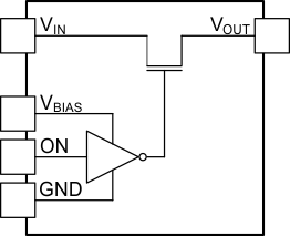
TPS22860 tps22860_fbd.gif

7.3 Feature Description

7.3.1 ON/OFF Control

The ON input controls the load switch with positive logic.

7.3.2 Pass Transistor

The TPS22860 supports up to 200-mA current flow in either direction. RON is dependent on VBIAS as shown in Figure 1, Figure 2, and Figure 3.

7.4 Device Functional Modes

Table 1. Functional Table

ON VIN to VOUT
L Off
H On