JAJSGL9C October 2013 – December 2018 TPS24750 , TPS24751
UNLESS OTHERWISE NOTED, this document contains PRODUCTION DATA.
- 1 特長
- 2 アプリケーション
- 3 概要
- 4 改訂履歴
- 5 Device Comparison Table
- 6 Pin Configuration and Functions
- 7 Specifications
- 8 Parameter Measurement Information
-
9 Detailed Descriptions
- 9.1 Overview
- 9.2 Functional Block Diagram
- 9.3 Feature Description
- 9.4 Device Functional Modes
-
10Application and Implementation
- 10.1 Application Information
- 10.2
Typical Application
- 10.2.1 Design Requirements
- 10.2.2
Detailed Design Procedure
- 10.2.2.1
Power-Limited Start-Up
- 10.2.2.1.1 STEP 1. Choose RSENSE, RSET, and RIMON
- 10.2.2.1.2 STEP 2. Choose Power-Limit Value, PLIM, and RPROG
- 10.2.2.1.3 STEP 3. Choose Output Voltage Rising Time, tON, and Timing Capacitor CT
- 10.2.2.1.4 STEP 4. Calculate the Retry-Mode Duty Ratio
- 10.2.2.1.5 STEP 5. Select R1, R2, and R3 for UV and OV
- 10.2.2.1.6 STEP 6. Choose R4, R5, and C1
- 10.2.2.2 Alternative Design Example: Gate Capacitor (dv/dt) Control in Inrush Mode
- 10.2.2.3 Additional Design Considerations
- 10.2.2.1
Power-Limited Start-Up
- 10.2.3 Application Curves
- 10.3 System Examples
- 11Power Supply Recommendations
- 12Layout
- 13デバイスおよびドキュメントのサポート
- 14メカニカル、パッケージ、および注文情報
パッケージ・オプション
メカニカル・データ(パッケージ|ピン)
- RUV|36
サーマルパッド・メカニカル・データ
- RUV|36
発注情報
10.2.2.1 Power-Limited Start-Up
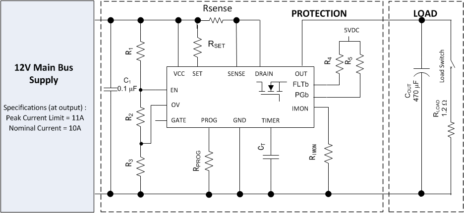
This design example assumes a 12-V system voltage with an operating tolerance of ±2 V. The rated load current is 10 A. If the current exceeds 11 A, then the device must shut down and then attempt to restart. Ambient temperatures may range from 20°C to 60°C. The load has a minimum input capacitance of 470 μF. The load is turned on only after the PG signal is asserted. Figure 41 shows a simplified system block diagram of the proposed application.
This design procedure seeks to control the junction temperature of device under both static and transient conditions by proper selection of current limit, fault timeout, and power limit. The design procedure assumes the worst case as a unit running at full load and maximum ambient temperature experiences a short circuit event. Adjust this procedure to fit the application and design criteria.
