JAJSGL9C October 2013 – December 2018 TPS24750 , TPS24751
UNLESS OTHERWISE NOTED, this document contains PRODUCTION DATA.
- 1 特長
- 2 アプリケーション
- 3 概要
- 4 改訂履歴
- 5 Device Comparison Table
- 6 Pin Configuration and Functions
- 7 Specifications
- 8 Parameter Measurement Information
-
9 Detailed Descriptions
- 9.1 Overview
- 9.2 Functional Block Diagram
- 9.3 Feature Description
- 9.4 Device Functional Modes
-
10Application and Implementation
- 10.1 Application Information
- 10.2
Typical Application
- 10.2.1 Design Requirements
- 10.2.2
Detailed Design Procedure
- 10.2.2.1
Power-Limited Start-Up
- 10.2.2.1.1 STEP 1. Choose RSENSE, RSET, and RIMON
- 10.2.2.1.2 STEP 2. Choose Power-Limit Value, PLIM, and RPROG
- 10.2.2.1.3 STEP 3. Choose Output Voltage Rising Time, tON, and Timing Capacitor CT
- 10.2.2.1.4 STEP 4. Calculate the Retry-Mode Duty Ratio
- 10.2.2.1.5 STEP 5. Select R1, R2, and R3 for UV and OV
- 10.2.2.1.6 STEP 6. Choose R4, R5, and C1
- 10.2.2.2 Alternative Design Example: Gate Capacitor (dv/dt) Control in Inrush Mode
- 10.2.2.3 Additional Design Considerations
- 10.2.2.1
Power-Limited Start-Up
- 10.2.3 Application Curves
- 10.3 System Examples
- 11Power Supply Recommendations
- 12Layout
- 13デバイスおよびドキュメントのサポート
- 14メカニカル、パッケージ、および注文情報
パッケージ・オプション
メカニカル・データ(パッケージ|ピン)
- RUV|36
サーマルパッド・メカニカル・データ
- RUV|36
発注情報
10.2.2.1.2 STEP 2. Choose Power-Limit Value, PLIM, and RPROG
The internal MOSFET dissipates large amounts of power during inrush. The power limit PLIM of the TPS2475x must be set to prevent the internal FET die temperature from exceeding a short-term maximum temperature, TJ(MAX)2. The short-term TJ(MAX)2 could be set ≤125°C to have sufficient margin to the internal maximum FET junction temperature. Equation 6 is an expression for calculating PLIM.

In the above equation, RθCA= RθJA – RθJC
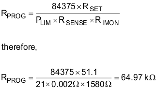
Where, RθCA is the case-to-ambient thermal resistance (RθCA is a strong function of the user defined PCB layout and heat sinking provided on Pad-2 of the device and can vary accordingly), RθJA is the junction-to-ambient thermal resistance and RθJC is the junction-to-case thermal resistance of the device, (In Equation 6 , the values are used from the TPS2475x Thermal Information table), rDS(on) is internal FET on-resistance at the maximum operating temperature, and the factor of 0.8 represents the tolerance of the constant-power engine. For an ambient temperature of 60°C, the calculated maximum PLIM is 33 W. Power limit selected must be lower than value obtained in Equation 6, to have substantial safe margin considering the tolerance of components and extended system temperatures. Power limit (PLIM) of 21 W is considered for this design. From Equation 1, a 64.9-kΩ, 1% resistor is selected for RPROG (see Equation 7).

Power Limit fold back (PLIM-FB) is the ratio of operating current (ILIM) and minimum power limited (regulated) current (when VOUT = 0V). Degradation of programmed power limit (PLIM) accuracy and start up issues may occur if PLIM-FB is too large. Equation 8 calculates VSNS-PL_MIN (minimum sense voltage during power limit) and PLIM-FB. To ensure reliable operation, verify that PLIM-FB < 12 and VSNS-PL_MIN ≥ 3mV.

If the above conditions are not met, please adjust and align RSENSE, PLIM set, and TA(MAX) appropriately to satisfy the above conditions.