JAJSGL9C October 2013 – December 2018 TPS24750 , TPS24751
UNLESS OTHERWISE NOTED, this document contains PRODUCTION DATA.
- 1 特長
- 2 アプリケーション
- 3 概要
- 4 改訂履歴
- 5 Device Comparison Table
- 6 Pin Configuration and Functions
- 7 Specifications
- 8 Parameter Measurement Information
-
9 Detailed Descriptions
- 9.1 Overview
- 9.2 Functional Block Diagram
- 9.3 Feature Description
- 9.4 Device Functional Modes
-
10Application and Implementation
- 10.1 Application Information
- 10.2
Typical Application
- 10.2.1 Design Requirements
- 10.2.2
Detailed Design Procedure
- 10.2.2.1
Power-Limited Start-Up
- 10.2.2.1.1 STEP 1. Choose RSENSE, RSET, and RIMON
- 10.2.2.1.2 STEP 2. Choose Power-Limit Value, PLIM, and RPROG
- 10.2.2.1.3 STEP 3. Choose Output Voltage Rising Time, tON, and Timing Capacitor CT
- 10.2.2.1.4 STEP 4. Calculate the Retry-Mode Duty Ratio
- 10.2.2.1.5 STEP 5. Select R1, R2, and R3 for UV and OV
- 10.2.2.1.6 STEP 6. Choose R4, R5, and C1
- 10.2.2.2 Alternative Design Example: Gate Capacitor (dv/dt) Control in Inrush Mode
- 10.2.2.3 Additional Design Considerations
- 10.2.2.1
Power-Limited Start-Up
- 10.2.3 Application Curves
- 10.3 System Examples
- 11Power Supply Recommendations
- 12Layout
- 13デバイスおよびドキュメントのサポート
- 14メカニカル、パッケージ、および注文情報
パッケージ・オプション
メカニカル・データ(パッケージ|ピン)
- RUV|36
サーマルパッド・メカニカル・データ
- RUV|36
発注情報
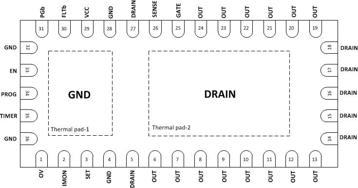
6 Pin Configuration and Functions
TPS24750, TPS24751 RUV Package
36-Pin VQFN
Top View

Pin Functions
| PIN | TYPE | DESCRIPTION | |
|---|---|---|---|
| NAME | NO. | ||
| DRAIN | 5, 14-18, 27 | I | The drain of the internal pass MOSFET. Connect to a terminal of current sense resistor in the power path |
| EN | 33 | I | Active high enable input. Logic input. Connects to resistor divider |
| FLTb | 30 | I | Active-low, open-drain output indicates overload fault timer has turned internal FET off |
| GATE | 25 | I/O | Gate driver output for the internal MOSFET |
| GND | 4, 28, 32, 36 | GND | Ground |
| IMON | 2 | O | Load current analog and current limit program point. Connect RIMON to ground |
| OUT | 6-13, 19-24 | I/O | Internally connect to the source of internal pass MOSFET. Connect to output capacitors and load |
| OV | 1 | I | Overvoltage comparator input. Connects to resistor divider. GATE is pulled low when OV exceeds the threshold |
| Pad-1 | — | — | Tied to GND |
| Pad-2 | — | — | Tied to DRAIN |
| PGb | 31 | O | Active-low, open-drain power good indicator. Status is determined by the voltage across the MOSFET |
| PROG | 34 | I | Power-limiting programming pin. A resistor from this pin to GND sets the maximum power dissipation for the internal pass MOSFET |
| SENSE | 26 | I | Current sensing input for resistor shunt from VCC to SENSE. Connect to a terminal of current sense resistor |
| SET | 3 | I | Current limit programming set pin. A resistor is connected from this pin to VCC |
| TIMER | 35 | I/O | A capacitor connected from this pin to GND provides a fault timing function |
| VCC | 29 | I | Input voltage sense and power supply |