SLUS660I September 2005 – January 2015 TPS40140
PRODUCTION DATA.
- 1 Features
- 2 Applications
- 3 Description
- 4 Revision History
- 5 Device Comparison Table
- 6 Pin Configuration and Functions
- 7 Specifications
- 8 Detailed Description
-
9 Application and Implementation
- 9.1
Application Information
- 9.1.1 Synchronizing a Single Controller to an External Clock
- 9.1.2 Split Input Voltage Operation
- 9.1.3 Configuring Single and Multiple ICs
- 9.1.4 Digital Clock Synchronization
- 9.1.5 Typical Start-Up Sequence
- 9.1.6 Track (Soft-Start Without PreBiased Output)
- 9.1.7 Soft-Start With PreBiased Outputs
- 9.1.8 Track Function in Configuring a Slave Channel
- 9.1.9 Differential Amplifier, U9
- 9.1.10 Setting the Output Voltage
- 9.1.11 Programmable Input UVLO Protection
- 9.1.12 CLKFLT, CLKIO Pin Fault
- 9.1.13 PHSEL Pin Fault
- 9.1.14 Overtemperature
- 9.1.15 Fault Masking Operation
- 9.1.16 Setting the Switching Frequency
- 9.1.17 Current Sense
- 9.1.18 Current Sensing and Balancing
- 9.1.19 Overcurrent Detection and Hiccup Mode
- 9.1.20 Calculating Overcurrent Protection Level
- 9.1.21 Design Examples Information
- 9.2
Typical Application
- 9.2.1
Application 1: Dual-Output Configuration from 12 to 3.3 V and 1.5 V DC-DC Converter Using a TPS40140
- 9.2.1.1 Design Requirements
- 9.2.1.2
Detailed Design Procedure
- 9.2.1.2.1 Step 1: Inductor Selection
- 9.2.1.2.2 Step 2: Output Capacitor Selection
- 9.2.1.2.3 Step 3: Input Capacitor Selection
- 9.2.1.2.4 Step 4: MOSFET Selection
- 9.2.1.2.5
Step 5: Peripheral Component Design
- 9.2.1.2.5.1 Switching Frequency Setting (RT Pin 5)
- 9.2.1.2.5.2 Output Voltage Setting (FB1 Pin 36)
- 9.2.1.2.5.3 Current Sensing Network Design (CS1 Pin 31 and CSRT1 Pin 32)
- 9.2.1.2.5.4 Overcurrent Protection (ILIM1 Pin 34)
- 9.2.1.2.5.5 VREG (Pin 21)
- 9.2.1.2.5.6 BP5 (Pin 8)
- 9.2.1.2.5.7 PHSEL (Pin 4)
- 9.2.1.2.5.8 VSHARE (Pin 6)
- 9.2.1.2.5.9 PGOOD1 (Pin 30)
- 9.2.1.2.5.10 UVLO_CE1 (Pin 29)
- 9.2.1.2.5.11 Clkio (Pin 28)
- 9.2.1.2.5.12 BOOT1 and SW1 (Pin 27 and 25)
- 9.2.1.2.5.13 TRK1 (Pin 33)
- 9.2.1.2.5.14 DIFFO, VOUT, and GSNS (Pin 1, Pin 2, and Pin 3)
- 9.2.1.2.6 Feedback Compensator Design (COMP1 Pin 35)
- 9.2.1.3 Application Curves
- 9.2.2
Application 2: Two-Phase Single Output Configuration from 12 to 1.5 V DC-DC Converter Using a TPS40140
- 9.2.2.1 Design Requirements
- 9.2.2.2
Detailed Design Procedure
- 9.2.2.2.1 Step 1: Output Capacitor Selection
- 9.2.2.2.2 Step 2: Input Capacitor Selection
- 9.2.2.2.3
Step 3: Peripheral Component Design
- 9.2.2.2.3.1 Switching Frequency Setting (Rt Pin 5)
- 9.2.2.2.3.2 COMP1 and COMP2 (Pin 35 and Pin 10)
- 9.2.2.2.3.3 TRK1 and TRK2 (Pin 33 and Pin 12)
- 9.2.2.2.3.4 ILIM1 and ILIM2 (Pin 34 and Pin 11)
- 9.2.2.2.3.5 FB1 and FB2 (Pin 36 and Pin 9)
- 9.2.2.2.3.6 PHSEL (Pin 4)
- 9.2.2.2.3.7 PGOOD1 and PGOOD2 (Pin 30 and Pin 15)
- 9.2.2.2.3.8 CLKIO (Pin 28)
- 9.2.2.2.3.9 DIFFO, VOUT, and GSNS (Pin 1, Pin 2, and Pin 3)
- 9.2.3 Application Curves
- 9.2.1
Application 1: Dual-Output Configuration from 12 to 3.3 V and 1.5 V DC-DC Converter Using a TPS40140
- 9.3
System Example
- 9.3.1
Four-Phase Single Output Configuration from 12 to 1.8 V DC-DC Converter Using Two TPS40140
- 9.3.1.1 Step 1: Output Capacitor Selection
- 9.3.1.2 Step 2: Input Capacitor Selection
- 9.3.1.3
Step 3: Peripheral Component Design
- 9.3.1.3.1
Master Module
- 9.3.1.3.1.1 Rt (Pin 5)
- 9.3.1.3.1.2 COMP1 and COMP2 (Pin 35 and Pin 10)
- 9.3.1.3.1.3 TRK1 and TRK2 (Pin 33 and Pin 12)
- 9.3.1.3.1.4 ILIM1 and ILIM2 (Pin 34 and Pin 11)
- 9.3.1.3.1.5 FB1 and FB2 (Pin 36 and Pin 9)
- 9.3.1.3.1.6 PHSEL (Pin 4)
- 9.3.1.3.1.7 PGOOD1 and PGOOD2 (Pin 30 and Pin 15)
- 9.3.1.3.1.8 CLKIO (Pin 28)
- 9.3.1.3.2
Slave Module:
- 9.3.1.3.2.1 RT (Pin 5)
- 9.3.1.3.2.2 COMP1 and COMP2 (Pin 35 and Pin 10)
- 9.3.1.3.2.3 TRK1 and TRK2 (Pin 33 and Pin 12)
- 9.3.1.3.2.4 ILIM1 and ILIM2 ( Pin 34 and Pin 11)
- 9.3.1.3.2.5 FB1 and FB2 (Pin 36 and Pin 9)
- 9.3.1.3.2.6 PHSEL (Pin 4)
- 9.3.1.3.2.7 PGOOD1 and PGOOD2 (Pin 30 and Pin 15)
- 9.3.1.3.2.8 CLKIO (Pin 28)
- 9.3.1.3.1
Master Module
- 9.3.1
Four-Phase Single Output Configuration from 12 to 1.8 V DC-DC Converter Using Two TPS40140
- 9.1
Application Information
- 10Power Supply Recommendations
- 11Layout
- 12Device and Documentation Support
- 13Mechanical, Packaging, and Orderable Information
9 Application and Implementation
NOTE
Information in the following applications sections is not part of the TI component specification, and TI does not warrant its accuracy or completeness. TI’s customers are responsible for determining suitability of components for their purposes. Customers should validate and test their design implementation to confirm system functionality.
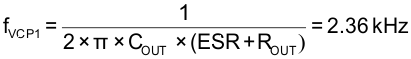
9.1 Application Information
The following sections are partitioned to facilitate applying the TPS40140 in various modes and configurations. The first sections describe functions that are used in all configurations. The following sections are specific to the configuration (that is, single controller, multiple controllers, master and slave).
9.1.1 Synchronizing a Single Controller to an External Clock
The TPS40140 has the ability to synchronize a single controller to an external clock. The clock must be a pulse stream at 6 or 8 times the master PWM frequency. See Figure 16.
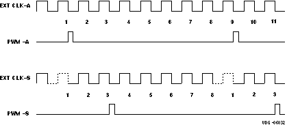 Figure 16. Synchronizing a Single Controller to an External Clock
Synchronizing the single controller to an external clock is similar to synchronizing a clock slave to a clock master. The single controller is put in clock slave mode by connecting the RT pin to BP5, disabling the internal clock generator. If the external CLKIO signal is a clock stream without any missing pulses, the master synchronize to an arbitrary pulse so there is no determinant phase synchronization. Without a missing pulse, the PWM frequency is 1/8 of the external clock. If the external CLKIO signal has a missing pulse every 6 cycles or 8 cycles, the controller synchronizes based on the missing pulse which would be in the 6th or 8th position. With the missing pulse, the phase synchronization of the master, to the missing pulse, can be controlled by the voltage on the PHSEL pin. See the section on DIGITAL CLOCK SYNCHRONIZATION. Phase shifting would also be desirable if more than one controller were to be synchronized to the same external clock. The high-level threshold for the external clock is 3.2 V, and the low-level threshold is 0.5 V. The typical duty ratio is approximately 0.5.
Figure 16 shows a time slice of the two external clock possibilities and the resulting PWM signal. EXT CLK-A is the continuous clock with no missing pulse and the PWM-A signal could be frequency synchronized anywhere in the clock stream. The PWM signal is at 1/8 of the EXT CLK-A frequency. EXT CLK-S is the external clock stream with a missing pulse every 8 cycles. The phasing of the PWM-S is based on the voltage on the PHSEL pin. For PHSEL grounded, the PWM-S signal is shifted 90 degrees from what would be the falling edge of the missing pulse as shown in Figure 16.
If the controller has free running operation (in clock master mode) before receiving the external clock, the switching frequency is set by connecting a resistor from the RT pin to GND. In order to receive the external clock, the PHSEL pin should be connected to GND to disable the output of CLKIO pin. A 500-Ω resistor is recommended to be placed between the external clock and the CLKIO pin. When dynamically shorting the RT pin to BP5 through a switch, the controller switches to clock slave mode and starts to synchronize to the external clock.
9.1.2 Split Input Voltage Operation
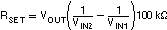
It may be advantageous to operate a master controller’s power stages from VIN1, different from the slave controller(s) power stages, VIN2 where VIN1 > VIN2. This enables the system designer to optimize the current taken from the system input voltages. In order to balance the output currents, a programmed offset is applied to ILIM2 of the slave controller(s). The voltage on this pin sets the offset current for channel 2.
The ramp offset is determined by a resistor, RSET, connected to the ILIM2 pin of the slave, and is given by:
9.1.3 Configuring Single and Multiple ICs
The controller may be configured for a single output, 2-phase mode or a dual output voltage mode. In the dual output mode the input voltages and the output voltages are independent of each other. In 2-phase mode the input voltages and output voltages are tied together, respectively and certain other pins must be configured. The two phases of a single controller are always 180° out-of-phase. The entry in Table 3 that refer to "TO NETWORK" means the normal resistor-capacitor network used for control loop compensation. The other entries refer to components that are typically connected to the device pin.
Table 2. Configuring Clock Mode
| TIMING RESISTANCE VOLTAGE (V) | CLOCK MODE |
|---|---|
| < 0.7 V (resistor to GND) | Master (or single device) |
| > 1 V (tied to VREG or VDD) | Slave |
9.1.3.1 Single Device Operation
A single controller may be configured as a 2-phase or dual output. A summary of the modes and device pin connections for a single controller is given in Table 3. The basic schematic of a single controller operating in a 2-phase mode is shown in Figure 17. The dual output schematic is shown in Figure 18.
Table 3. TPS40140 Single Device Mode Selection and Pin Configuration
| DEVICE PIN | FOR 2 PHASE MODE | FOR DUAL OUTPUT MODE |
|---|---|---|
| COMP1 | TO NETWORK | TO NETWORK |
| COMP2 | COMP1 | TO NETWORK |
| TRK1 | TO SS CAPACITOR | TO SS CAPACITOR |
| TRK2 | TO BP5 | TO SS CAPACITOR |
| ILIM1 | TO SET RESISTORS | TO SET RESISTORS |
| ILIM2 | GND | TO SET RESISTORS |
| FB1 | TO NETWORK | TO NETWORK |
| FB2 | GND | TO NETWORK |
| PHSEL | GND | GND |
| PGOOD1 | TO PULLUP RESISTOR | TO PULL-UP RESISTOR |
| PGOOD1 | TO PULLUP RESISTOR | TO PULL-UP RESISTOR |
| CLKIO | OPEN | OPEN |
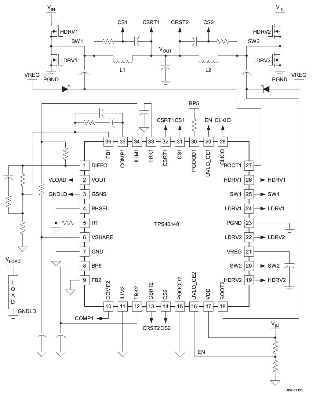 Figure 17. Typical Applications Circuit, 2-Phase Mode
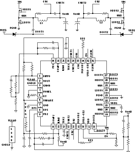 Figure 18. Typical Applications Circuit, Dual Mode
9.1.3.2 Multiple Devices
In a multiple device system, it is often desirable to synchronize the clocks each device to minimize input ripple current as well as radiated and conducted emissions. This is accomplished by designating one of the controllers as the master and the other devices as 'slaves. The master generates the system clock, CLKIO, and it is distributed to the slaves. This is the most useful configuration of multiple devices and the one that is demonstrated in this data sheet. It is described in more detail in the Clock Master, PHSEL, and CLKIO Configurations section.
To increase the total current capability, or number of outputs, a single slave controller can be added to a master controller as shown in Figure 21. The configuration of the 2-phase master and a 2-phase slave controller is also shown in Table 4 It is possible to have the master controller operate on one switching frequency and the slave controllers on another, independent frequency. In a multi-phase system the slave controllers would continue to share load current with the master. This is not a preferred configuration and is mentioned here only for completeness.
The 10-kΩ resistor connected from the CLKIO line to GND is required to ensure that the CLKIO line falls to GND quickly when the master device is shutdown or powers off. The master CLKIO pin goes to a high impedance state at these times and if the CLKIO line was high, there is no other active discharge part. The slave controllers look at the CLKIO line to determine if the system is supposed to be running or not. A level below 0.5 V on CLKIO is required for this purpose.
NOTE
In any system configured to have a CLK master and CLK slaves, a 10-kΩ resistor connected from CLKIO to GND is required.
Table 4. TPS40140 Two-Device, 4-Phase Mode Selection and Pin Configuration
| DEVICE PIN, MASTER | MASTER, 2-PHASE | DEVICE PIN, SLAVE | SLAVE, 2-PHASE |
|---|---|---|---|
| COMP1 | TO NETWORK | COMP1 | TO MASTER, COMP1 |
| COMP2 | COMP1 | COMP2 | TO MASTER, COMP1 |
| TRK1 | TO SS CAPACITOR | TRK1 | TO BP5 |
| TRK2 | TO BP5 | TRK2 | TO BP5 |
| ILIM1 | TO SET RESISTORS | ILIM1 | GND |
| ILIM2 | GND | ILIM2 | GND |
| FB1 | TO NETWORK | FB1 | GND |
| FB2 | GND | FB2 | GND |
| PHSEL | 39-kΩ TO GND | PHSEL | GND |
| PGOOD1 | TO PULLUP RESISTOR | PGOOD1 | TO PULL-UP RESISTOR |
| PGOOD1 | TO PULLUP RESISTOR | PGOOD1 | TO PULL-UP RESISTOR |
| CLKIO | TO SLAVE, CLKIO | CLKIO | TO MASTER, CLKIO |
| VSHARE | TO SLAVE, VSHARE | VSHARE | TO MASTER, VSHARE |
| BP5 | TO SLAVE, BP5 | BP5 | TO MASTER, BP5 |
DESIGN HINT
TI recommends adding a 220-pF ceramic capacitor in parallel with the PHSEL resistor string. This capacitor is connected from the PHSEL pin of the master control to GND.
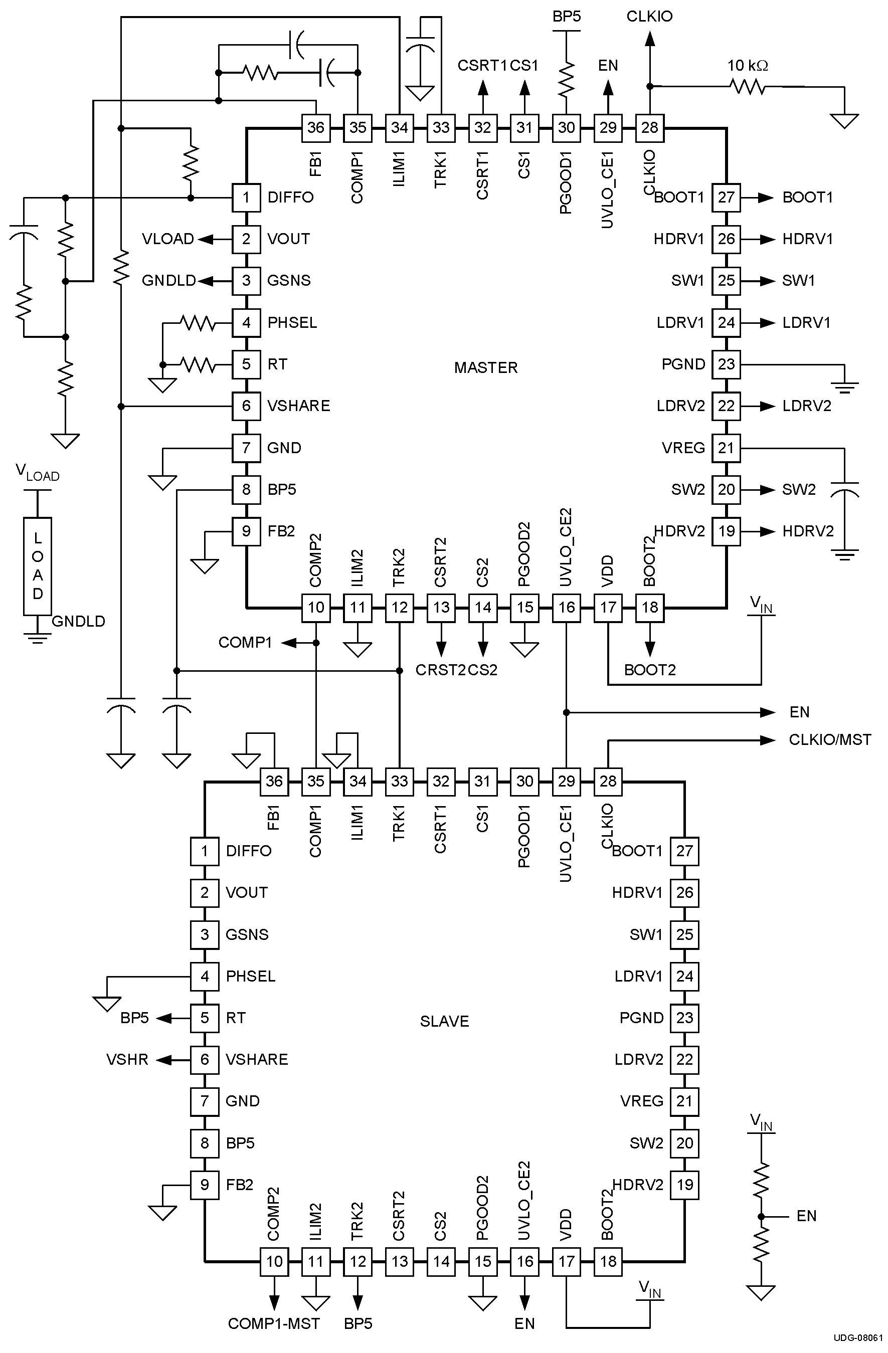 Figure 19. Typical Applications Circuit, 4-Phase Mode
In this configuration, the master senses that there is one slave controller, by the 39-kΩ resistor on the PHSRL pin, and distributes the CLKIO signal. The slave controller senses the 0-V level on its PHSEL pin and delays the proper number of CLKIO pulses to be 90° out-of-phase with the master.
Two ICs could also be configured as a 2-phase, single output master and a slave which has two independent outputs, but is synchronized with the master controller clock. Table 5 shows the configuration.
Table 5. TPS40140 Two-Device, 2-Phase Master and a Dual-Output Slave Configuration
| DEVICE PIN, MASTER | MASTER, 2 PHASE | DEVICE PIN, SLAVE | SLAVE, DUAL OUTPUT |
|---|---|---|---|
| COMP1 | To network | COMP1 | To network |
| COMP2 | COMP1 | COMP2 | To network |
| TRK1 | To SS capacitor | TRK1 | To SS capacitor |
| TRK2 | To BP5 | TRK2 | To SS capacitor |
| ILIM1 | To set resistors | ILIM1 | To set resistors |
| ILIM2 | GND | ILIM2 | To set resistors |
| FB1 | To network | FB1 | To network |
| FB2 | GND | FB2 | To network |
| PHSEL | 39-kΩ to GND | PHSEL | GND |
| PGOOD1 | To pullup resistor | PGOOD1 | To pullup resistor |
| PGOOD1 | To pullup resistor | PGOOD1 | To pullup resistor |
| CLKIO | To slave, CLKIO | CLKIO | To master, CLKIO |
9.1.3.3 Clock Master, PHSEL, and CLKIO Configurations
The clock synchronization between the master and the slave controller(s) is implemented in a simple configuration of series 39-kΩ resistors. There is a 20-μA current source from the PHSEL pin of the master controller. Depending on the number of slave controllers connected, the slave controllers selects the proper delay from the master CLKIO signal to accomplish phase interleaving. On a given master or slave controller, the two phases are always 180° out-of-phase.
The CLKIO signal has either six or eight clocks for each cycle of the switching period.
For maximum flexibility the master and slave controllers can be either in a 2-phase configuration or a Dual output configuration
9.1.3.3.1 One Device Operation
The basic configuration of a single device is shown in Figure 20.
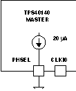 Figure 20. Single Controller Only, Two Phases
9.1.3.3.2 Two ICs Operation
To increase the total current capability, or number of outputs, a single slave controller can be added as shown in Figure 21.
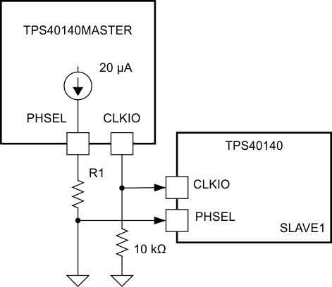 Figure 21. Master Controller and One Slave Controller, Four Phases
In this configuration, the master senses that there is one slave controller, and distributes the CLKIO signal. The slave controller senses the zero-volt level on its PHSEL pin and delays the proper number of CLKIO pulses to be 90° out-of-phase with the master.
9.1.3.3.3 Three ICs Operation
To increase the total current capability to six phases, or to increase the number of outputs, two slave controllers can be added as shown in Figure 22. In this configuration for perfect interleaving, the master and slaves are 120° out-of-phase. The CLKIO signal has six clocks for each cycle of the switching period; therefore, the switching period is reduced. In this six-phase mode, the switching frequency is increased 33%.
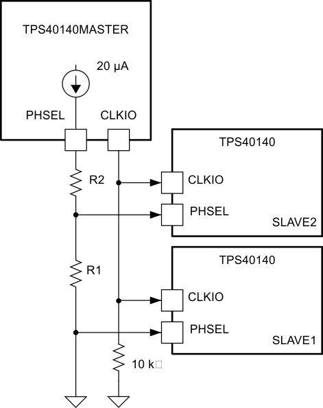 Figure 22. Master Controller and Two Slave Controllers, Six Phases
In this configuration, the master senses that there are two slave controllers, and distributes a six-phase CLKIO signal. The slave controllers sense the voltage on their PHSEL pins, and delay the proper number of CLKIO pulses to be 60° or 120° out-of-phase with the master.
9.1.3.3.4 Four ICs Operation
To further increase the total current capability to eight phases, or to increase the number of outputs, three slave controllers can be added as shown in Figure 23.
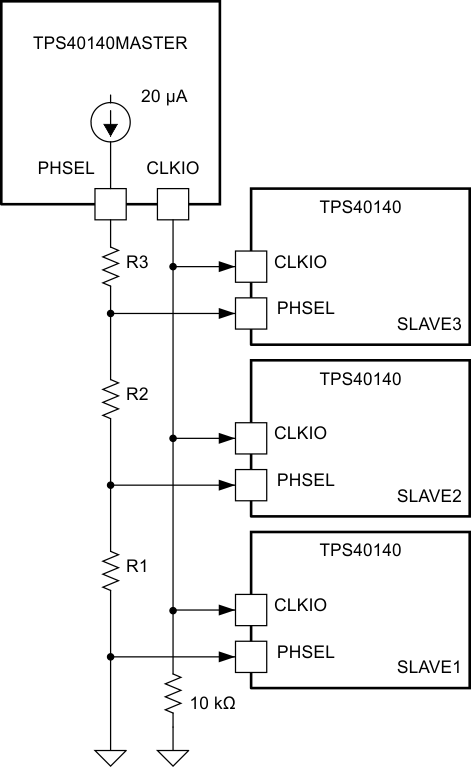 Figure 23. Master Controller and Three Slave Controllers, Eight Phases
In this configuration, the master senses that there are three slave controllers, and distributes a eight-phase CLKIO signal. The slave controllers sense the voltage on their PHSEL pins and delay the proper number of CLKIO pulses to be 45°, 90°, and 135° out-of-phase with the master.
9.1.3.3.5 Six ICs Operation
To further increase the total current capability to twelve phases, or to increase the number of outputs, five slave controllers can be added as shown in Figure 24.
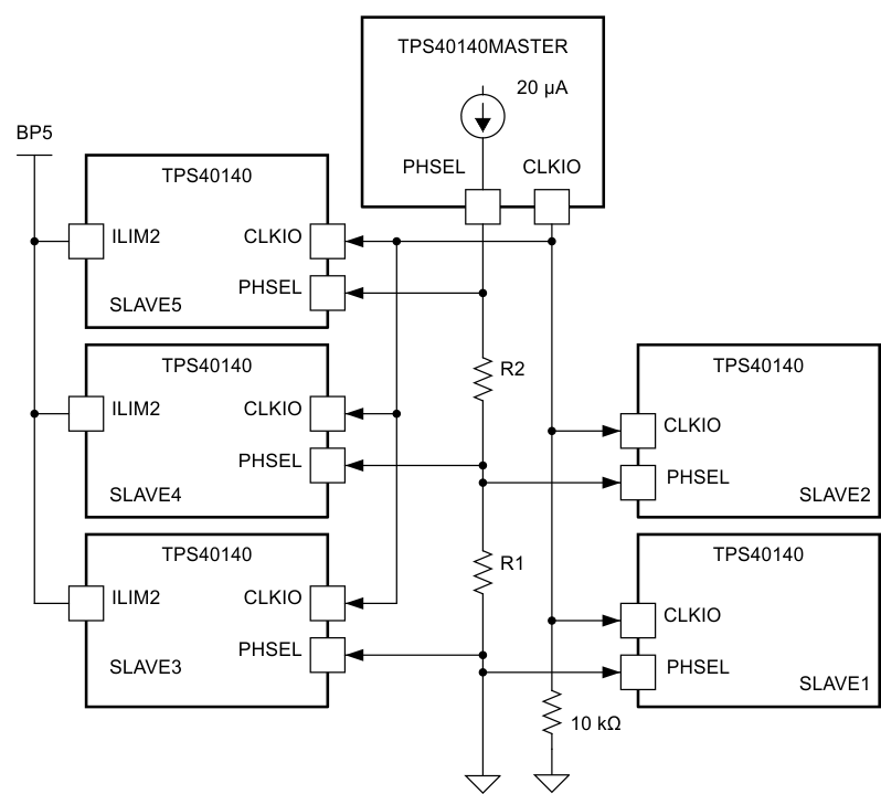
In this configuration, the master senses that there are two slave controllers (due to the 2 resistors) and distributes a six-phase CLKIO signal. Slave1 and slave2 are turned on at 60° and 120° respectively, as before with two slaves. However, to get twelve phases with a six-phase clock, both edges of the CLKIO signal are used to control the slaves. With the ILIM2 tied high on slave3,slave4, and slave5, they turn on at the rising edge of CLKIO while the master and slave1 and slave2 turn on at the falling edge of CLKIO.
If four slaves are desired, just delete one of the slaves from Figure 24. The interleaving is not perfect because there is be 30° between the master and three slaves. The deleted slave causes 60° between the two adjacent slaves. See Figure 26 for phasing details.
9.1.3.3.6 Eight ICs Operation
To further increase the total current capability to sixteen phases, or to increase the number of outputs, seven slave controllers can be added as shown in Figure 25.
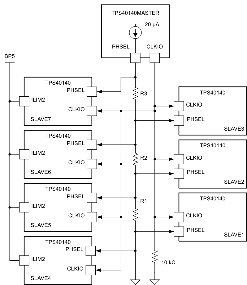
In this configuration, the master senses that there are three slave controllers (due to the three resistors) and distributes an eight-phase CLKIO signal. Slave1, slave2, and slave3 are turned on at 90°, 45°, and 135° respectively as before with three slaves. However, to get sixteen phases with an eight-phase clock, both edges of the CLKIO signal are used to control the slaves. With the ILIM2 tied high on slave4, slave5, slave6, and slave7 they turn on at the rising edge of CLKIO, while the master and slave1, slave2, and slave3 turn on at the falling edge of CLKIO. If six slaves are desired, just delete one of the slaves from Figure 25. The interleaving is not be perfect because there is 22.5° between the master and three slaves. The deleted slave causes 45° between the two adjacent slaves. See Figure 26 for a phasing details.
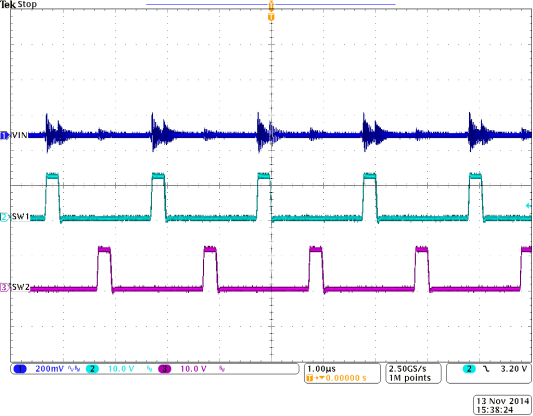
9.1.4 Digital Clock Synchronization
Figure 26 is a summary of the master and slave clock phasing. The master and the slaves can be selected to be a multi-phase, single output configuration and/or several independent output voltage rails, independent of the clocking.
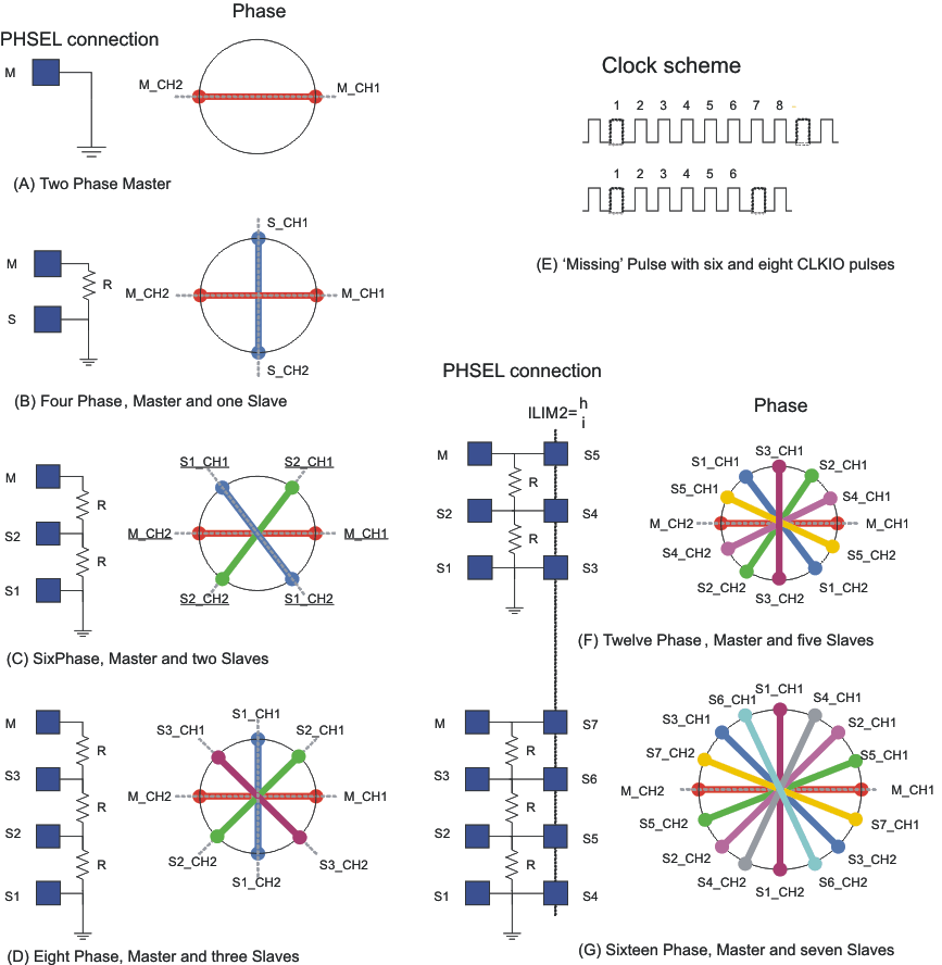 Figure 26. Clock Phasing Summary
9.1.4.1 Basic Configurations for 2, 4, 6, 8, 12, or 16 Phases
The solid square boxes in Figure 26 represent the PHSEL pin of the master (M) controller or a numbered slave controller (S1-S7). The labels on the spokes of the wheels indicate a master Channel 1 and master Channel 2 (M_CH1 and M_CH2) and numbered slaves Channel 1 and slave Channel 2 (Sn_CH1 and Sn_CH2). The Channel 1 and Channel 2 of a given master or slave is always 180° out-of-phase.
The master and slaves are automatically configured for proper phasing based on the resistor string from the master to the slaves. All the resistors are 39 kΩ to 41.2 kΩ. Part (A) above shows a single controller operating two phases 180° out-of-phase. Part (B) above shows four phase operation. This is configured by connecting a single resistor from the master PHSEL to GND and grounding the slave PHSEL pin. The individual channels are 90° out-of-phase. Part (C) above shows six phase operation. This is configured by connecting two resistors from the master PHSEL to GND. The first resistor tap is connected to slave2 PHSEL pin and then grounding the slave1 PHSEL pin. The individual channels are 60°out-of-phase. Part (D) above shows eight phase operation. This is configured by connecting three resistors from the master PHSEL to GND. The first resistor tap is connected to slave3 PHSEL pin. The second resistor tap is connected to slave2 PHSEL pin and then grounding the slave1 PHSEL pin. The individual channels are 45° out-of-phase. Part (F) above shows twelve phase operation. This is configured by connecting two resistors from the master PHSEL to GND. The master PHSEL pin is also connected to slave5 PHSEL pin. The first resistor tap is connected to slave2 and slave4 PHSEL pins and then grounding the slave1 and slave3 PHSEL pins. The individual channels are 30° out-of-phase. Additionally, the ILIM2 pins of slave5, slave4 and slave3 are left open (internal pullup) or externally connected to BP5. Part (G) above shows sixteen phase operation. This is configured by connecting three resistors from the master PHSEL to GND. The master PHSEL pin is also connected to slave7 PHSEL pin. The first resistor tap is connected to slave3 and slave6 PHSEL pins. The second resistor tap is connected to slave2 and slave5 PHSEL pins and then grounding the slave1 and slave4 PHSEL pins. The individual channels are 22.5° out-of-phase. Additionally, the ILIM2 pins of slave7, slave6, slave5, and slave4 are left open (internal pullup) or externally connected to BP5.
9.1.4.2 Configuring for Other Number of Phases
Configuring for other than 2, 4, 6, 8, 12 or 16 phases is simply a matter of not attaching one or more slave controllers. The phasing between master and populated slaves is as shown above. For example a 3-phase system could be configured with a master CH1 and master CH2 and 1 phase of a slave. Referring to Part (B) above, the 3 phases could be master CH1, master CH2 and slave CH1 or slave CH2 as shown in Figure 27.
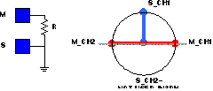 Figure 27. Phase System: 2 Channels of the Master and 1 Channel of the Slave
The 3-phase system could also be configured with 1 channel of the master and 2 channels of the slave. Referring to Part (B) above, the 3 phases could be master CH1 or master CH2 and slave CH1 and slave CH2. In either of these configurations there is 90° between two of the channels and 180° between the other channel. The unused channel could be another independent output voltage whose clocking would occupy the phase not used in the 3-phase system. This philosophy can be used for any number of phases not shown in Figure 26, Clock Phasing Summary.
For example, a 10-phase system could be configured as shown in Figure 28.
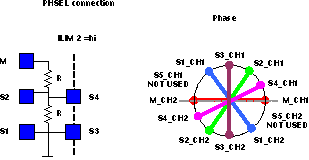 Figure 28. Ten-Phase System With Slaves Not Attached
Clocking between the attached slave channels is as shown.
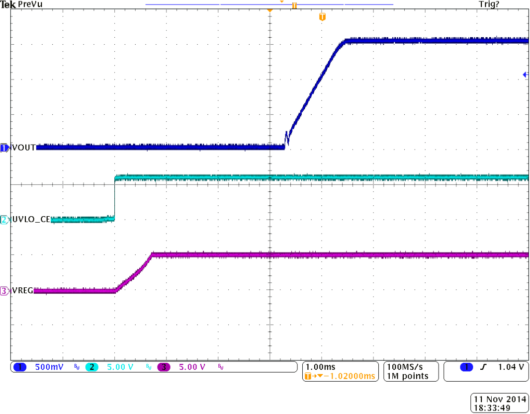
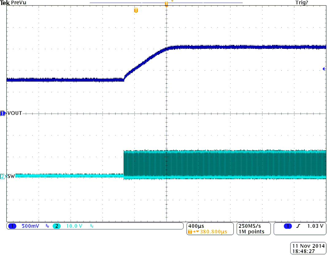
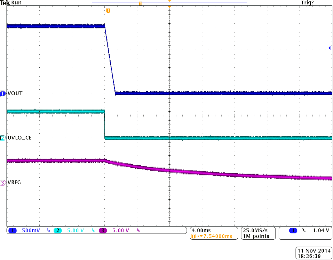
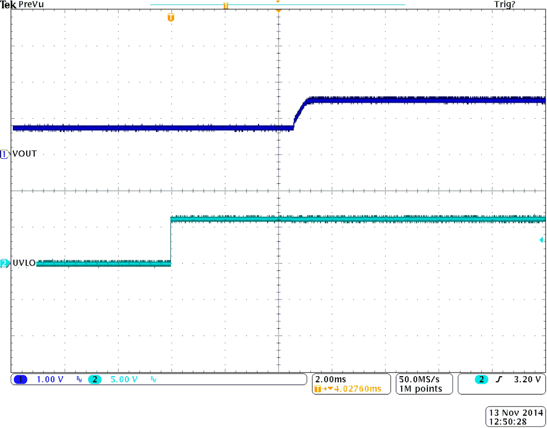
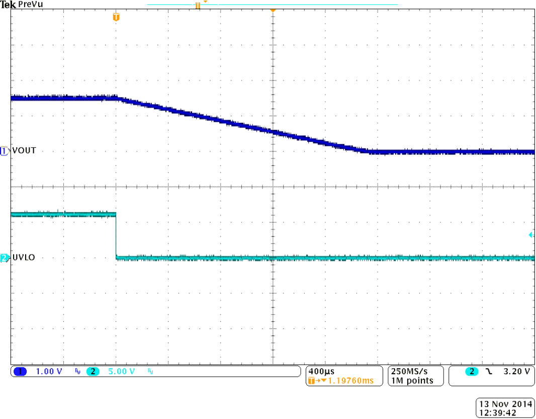
9.1.5 Typical Start-Up Sequence
Figure 29 shows a typical start-up with the VDD applied to the controller and then the UVLO-CEx being enabled. Shutdown occurs when the VDD is removed.
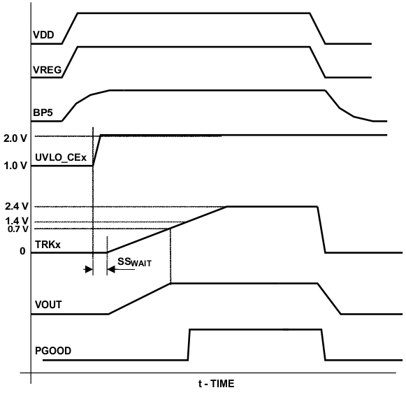 Figure 29. Typical Start-Up and Shut-Down Sequence
9.1.6 Track (Soft-Start Without PreBiased Output)
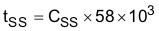
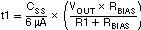
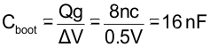
A capacitor connected to the TRKx pins sets the power-up time. When UVLO_CEx is high and the internal power-on reset (POR) is cleared, the calibrated current source, starts charging the external soft start capacitor with 12-μA. The PGOOD pin is held low during the start-up. The rising voltage across the capacitor serves as a reference for the error amplifier, U10 and U14. When the soft start voltage reaches the level of the reference voltage, VREF = 0.7 V, the converter’s output reaches the regulation point and further voltage rise of the soft-start voltage has no effect on the output. When the soft start voltage reaches 1.4 V, the powergood (PGOOD) function is cleared to be reported on the PGOOD pin. Normally the PGOOD pin goes high at this time. Equation 2 is used to calculate the value of the soft-start capacitor. CSS is in Farads and tSS is given in seconds.
9.1.7 Soft-Start With PreBiased Outputs
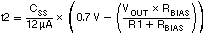
For prebiased outputs the TPS40140 uses two levels of soft-start current that charge the soft-start capacitor connected to the TRKx pin(s). PWM switching begins when the TRKx voltage rises to the voltage present on the FBx pin. When the first PWM pulse occurs, the charging current is increased to 12 μA. Figure 30 shows the typical waveforms present on the TRKx pin and the output voltage, VOUT when VOUT is prebiased. TRKx rises due to the 6 μA current, until at 1 the voltage on TRKx equals the prebiased voltage on the FBx pin, at time t1. At this time, the soft-start current is increased to 12 μA and TRKx rises with an increase in the slope. When TRKx reaches 0.7 V, at time t2, the output should be in regulation. The voltage on the TRKx pin continues to rise. When the TRKx voltage is 1.4 V, at time t3, the PGOODx signal is enabled. The TRKx voltage continues to rise to 2.4 V where it is clamped internally. This approach provides for an accurate detection of the threshold where FBx = TRKx. Figure 31 is a block diagram of the implementation. The calculation for the soft start time, due to prebias, includes the time from t0 to t1, plus the time from t1 to t2, as shown in Equation 3 through Equation 5.
where
- CSS is in Farads
- tSS is in seconds

If there is no prebias (VOUT = 0 V), the equation reduces to case without prebias.
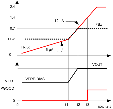 Figure 30. Soft-Start With PreBiased Output Waveforms
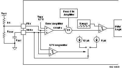 Figure 31. Implementation of PreBiased Output
DESIGN HINT
If the prebiased is greater than the regulation voltage, the controller does not start. This is a condition of an overvoltage being applied before the controller starts PWM switching.
9.1.8 Track Function in Configuring a Slave Channel
The TRKx pin is internally clamped to 2.4 V. To configure a channel as a slave, the TRKx pin is pulled up externally to 5 V. This configures the output of the error amplifier, COMPx, for that channel to be a high impedance, allowing the master COMP signal to control the slave channel.
9.1.9 Differential Amplifier, U9
The unity gain differential amplifier has high bandwidth to achieve improved regulation at user defined point of load and ease layout constrains. The output voltage is sensed between the VOUT and GSNS pins. The output voltage programming divider is connected to the output of the amplifier, the DIFFO pin.
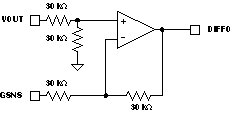 Figure 32. Differential Amplifier Configuration
DESIGN HINT
Because of the resistor configuration of the differential amplifier, the input impedance must be kept very low or errors result in setting the output voltage.
9.1.10 Setting the Output Voltage
Two resistors, R1 and RBIAS sets the output voltage as shown in Figure 33.
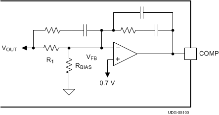
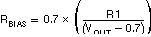
RBIAS is calculated in Equation 6.
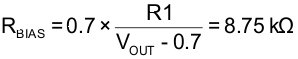
9.1.11 Programmable Input UVLO Protection
A voltage divider that sets 2 V on the UVLO_CEx pins determines when the controller begins to operate. The internal regulators are enabled when the voltage on the UVLO_CEx pins exceeds 1 V, but switching commences when the voltage is 2 V.
9.1.12 CLKFLT, CLKIO Pin Fault
If the CLKIO signal is to be distributed from the master to the slave controllers, and is not there, the slave controller enters a ‘Standby’ mode. The upper and lower MOSFETs are turned off but the internal 5-V regulator is still active and VREG is present. The CLKIO signal could be turned off at the master controller or the connection to the slave CLKIO input could be opened. If the CLKIO signal is restored, normal operation continues.
9.1.13 PHSEL Pin Fault
The PHSEL pin is normally terminated with a resistor string, or tied directly to ground. If this string becomes open, the PHSEL pin voltage is pulled up internally to greater than 4 V. The controller enters a ‘Standby’ mode. The upper and lower MOSFETs are turned off but the internal 5-V regulator is still active and VREG is present. If the PHSEL connection is restored, normal operation continues after 64 PWM clock cycles.
9.1.14 Overtemperature
If the temperature of the controller die is detected to be above 155°C, the upper and lower MOSFETs are turned off and the 5-V regulator, VREG, is turned off. When the die temperature decreases 30°C the controller performs a normal start-up.
9.1.15 Fault Masking Operation
If the TRKx pin voltage is externally limited below the 1.4-V threshold, the controller does not respond to an Undervoltage fault and the PGOOD output remains low. Other fault modes remain operational. The overcurrent protection continues to terminate PWM cycle every time the threshold is exceeded, but the hiccup mode is not entered.
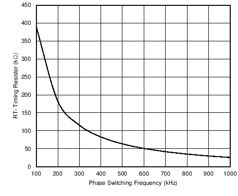
9.1.16 Setting the Switching Frequency
The clock frequency is programmed by the value of the timing resistor connected from the RT pin to ground. See Equation 7. This equation gives the frequency for an 8-phase system. For a 6-phase system the frequency is 1 1/3 times higher.
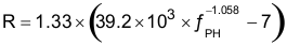
where
- ƒPH is a single-phase frequency, kHz
- The Rt resistor value is expressed in kΩ
See Figure 34.
9.1.17 Current Sense
Figure 35 shows the current sensing and overcurrent detection architecture.
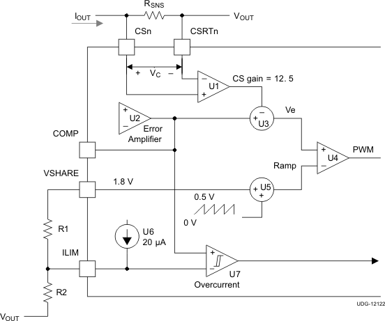 Figure 35. Output Current Sensing and Overcurrent Detection
The output current, IOUT, flows through RSNS and develops a voltage, VC across it, representative of the output current. The voltage, VC, could also be derived from an R-C network in parallel with the output inductor. This voltage is amplified with a gain of 12.5 and then subtracted from the Error Amp output, COMP, to generate the Ve voltage. The Ve signal is compared to the slope-compensation RAMP signal to generate the PWM for the modulator. As the output current is increased, the amplified VC causes the Ve signal to decrease. In order to maintain the proper duty cycle (PWM), the COMP signal must increase. Therefore the magnitude of the COMP signal contains the output current information:

This is integral in the overcurrent detection as can be seen at comparator U7, comparing the ILIM voltage with COMP. In order to have the proper duty cycle at PWM, Ve is shown in Equation 9.
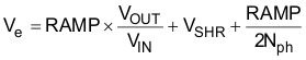
where
- Nph is 6 if PHSEL voltage = 1.6 ± 0.2 V, otherwise Nph is 8
Combining equations:
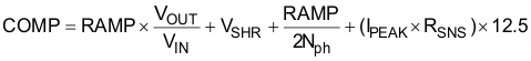
Equation 10 shows the reason for resistors R1 and R2 being tied to VSHR and VOUT, respectively.
9.1.18 Current Sensing and Balancing
The controller employs peak current mode control scheme, thus naturally provides certain degree of current balancing. With current mode, the level of current feedback should comply with certain guidelines depending on duty factor known as “slope compensation” to avoid the sub-harmonic instability. This requirement can prohibit achieving a higher degree of phase current balance. To avoid the controversy, a separate current loop that forces phase currents to match is added to the proprietary control scheme. This effectively provides high degree of current sharing independent of the controller’s small signal response and is implemented in U3 and U22 in the Functional Block Diagram section.
High bandwidth current amplifiers, U2 and U21 can accept as an input voltage either the voltage drop across dedicated precise current sense resistors, or inductor’s DCR voltage derived by an RC network, or thermally compensated voltage derived from the inductor’s DCR. The wide range of current sense arrangements ease the cost/complexity constrains and provides superior performance compared to controllers utilizing the low-side MOSFET current sensing.
See the Inductor DCR Current Sense section for selecting the values of the RC network.
9.1.19 Overcurrent Detection and Hiccup Mode
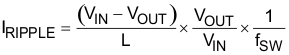
To reduce the input current and component dissipation during on overcurrent event, a hiccup mode is implemented. Hiccup mode refers to a sequence of 7 soft-start cycles where no MOSFET switching occurs and then a restart is attempted. If the fault has cleared, the restart results in returning to normal operation and regulation. This is shown in Figure 36.
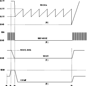 Figure 36. Hiccup Mode and Recovery
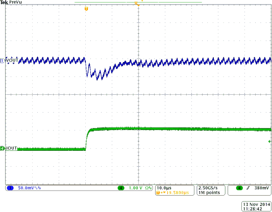
In Figure 36, normal operation is occurring between t0 and t1 as shown by VOUT being at the regulated voltage, (C) and normal switching on the SW NODE (B) and COMP at its nominal level, (D). At t1, an overcurrent load is experienced. The increased current forces COMP to increase to the ILIM level as shown in (D). If the COMP voltage is above the ILIM voltage for 7 switching cycles, the controller enters a hiccup mode. During this time the controller is not switching and the switching MOSFETs are turned off. The TRKx voltage goes through 7 cycles of charging and discharging the soft-start capacitor. At the end of the 7 cycles the controller attempts another normal restart. If the fault has been cleared, the output voltage comes up to the regulation level as shown at time t3. If the fault has not cleared, the COMP voltage again rises above the ILIM voltage and the hiccup mode repeats.
If the overcurrent condition exists for seven (7) PWM clock cycles the converter turns off the upper and lower MOSFETs and initiates a hiccup mode restart. In hiccup mode, the TRKx pin is periodically charged and discharged. After seven hiccup cycles, the controller attempts another soft-start cycle to restore normal operation. If the overload condition persists, the controller returns to the hiccup mode. This condition may continue indefinitely.
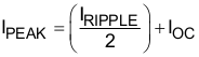
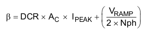
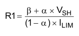
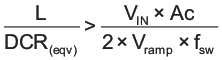
9.1.20 Calculating Overcurrent Protection Level
In order to set the desired overcurrent (IOC), a few variables must be known. The input and output voltage, the output inductor value and it's DC resistance (DCR), as well as the switching frequency. Also known are the ramp voltage which is 0.5 V and the VSHARE voltage, VSH which is 1.8 V. See the list of variables and their values at the end of this section.
The overcurrent set point is in terms of the DC output current, but the current sense circuit monitors the peak of the current. Therefore, the current ripple is needed and is calculated from the values of:
- input voltage (VIN)
- output voltage (VOUT)
- switching frequency (fSW)
- output inductance (L)
The ripple current is given by Equation 11.
Equation 12 calculates the detected peak current and is used in Equation 14.
It is this IPEAK current that is detected by the current sense circuit. The two resistors needed to set the peak overcurrent protection threshold and their connection for each channel is shown in Figure 37.
DESIGN HINT
Resistor R2 may be connected to the output voltage, VOUT, or to the output of the differential amplifier, DIFFO, if used.
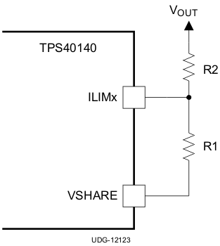 Figure 37. Selecting Overcurrent Threshold Resistors, R2 and R1
The two factors, alpha and beta help simplify the final equations and are given by Equation 13 and Equation 14.

R1 is shown in Equation 15.
R2 is shown in Equation 16.
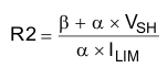
where
- VRAMP is the ramp amplitude (0.5 V typ)
- VIN is the input voltage
- DCR is the inductor equivalent DC resistance
- AC is the gain transfer to comparator
- IOC is the single-phase DC overcurrent trip point
- IPEAK is the peak single-phase inductor current
- Nph is 6 if PHSEL voltage = 1.6 V ±0.2 V, otherwise Nph = 8
- VSH is the VSHARE reference voltage (typ 1.8 V)
- ILIM is the current limit, output current (typ 20 μA)
- Variable range is specified in the Electrical Characteristics table
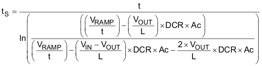
9.1.21 Design Examples Information
9.1.21.1 Inductor DCR Current Sense
The preferred method for sampling the output current for the TPS40140 is known as the inductor DCR method. This is a lossless approach, as opposed to using a discrete current sense resistor which occupies board area and impacts efficiency as well. The inductor DCR implementation is shown in Figure 38.
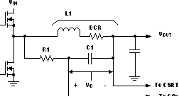 Figure 38. Inductor DCR Current Sense Approach
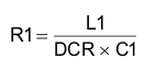
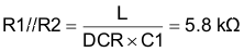
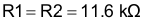
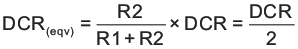
The inductor L1 consists of inductance, L, and resistance, DCR. The time constant of the inductor: L / DCR should equal the R1 × C1 time constant. Then choosing a value for C1 (0.1 μF is a good choice) solving for R1 is shown in Equation 17.
The voltage into the current sense amplifier of the controller , VC, is calculated in Equation 18.
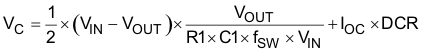
As the DC load increases the majority of the voltage, VC, is determined by (IOC ×DCR), where IOC is the per phase DC output current. It is important that at the overcurrent set point that the peak voltage of VC does not exceed 60 mV, the maximum differential input voltage. If the voltage VC exceeds 60 mV, a resistor, R2,can be added in parallel with C1 as shown in Figure 39. Adding R2 reduces the equivalent inductor DCR by the ratio shown in Equation 20
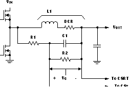 Figure 39. Using Resistor R2 to Reduce the Current Sense Amplifier Voltage
The parallel combination of R1 and R2 is shown in Equation 19.
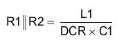
The ratio shown in Equation 20 provides the required voltage attenuation.

9.2 Typical Application
9.2.1 Application 1: Dual-Output Configuration from 12 to 3.3 V and 1.5 V DC-DC Converter Using a TPS40140
Figure 40 shows the schematic of the dual output converter design.
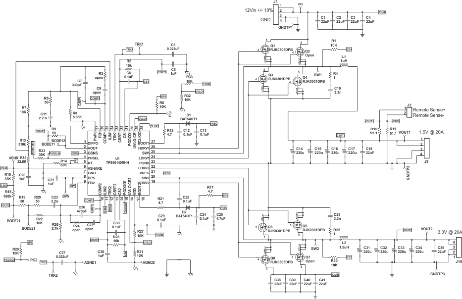 Figure 40. Dual-Output Converter Schematic
9.2.1.1 Design Requirements
The following example shows the design process and component selection for a dual output synchronous buck converter using TPS40140. Table 6 provides the design goal parameters. Only the calculated numbers for the 1.5-V output are shown, however, the equations are suitable for both channel design. A list of symbol definitions is found at the end of this section.
Table 6. Design Goal Parameters
| PARAMETER | TEST CONDITION | MIN | TYP | MAX | UNIT | |
|---|---|---|---|---|---|---|
| VIN | Input voltage | 10.8 | 12 | 13.2 | V | |
| VIN(ripple) | Input ripple voltage | IOUT = 20 A | 0.15 | V | ||
| VOUT | Output voltage | 1.5 | V | |||
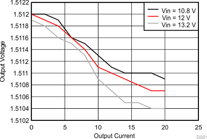
| Line regulation | 10.8 V ≤ VIN ≤ 13.2 V | 0.5% | ||||
| Load regulation | 0 V ≤ IOUT ≤ 20 A | 0.5% | ||||
| VP-P | Output ripple voltage | IOUT = 20 A | 30 | mV | ||
| ΔVOUT | Output voltage deviation during load transient | ΔIOUT = 10 A, VIN = 12 V | 80 | mV | ||
| IOUT | Output current | 10.8 V ≤ VIN ≤ 13.2 V | 0 | 20 | A | |
| η | Efficiency | IOUT = 20 A VIN = 12 V | 87% | |||
| fSW | Switching frequency | 500 | kHz | |||
9.2.1.2 Detailed Design Procedure
9.2.1.2.1 Step 1: Inductor Selection
The inductor is determined by the desired ripple current. The required inductor is calculated by:
Typically the peak-to-peak inductor current, IRIPPLE is selected to be around 20% of the rated output current. In this design, IRIPPLE is targeted at 15% of IOUT1. The calculated inductor is 0.89 μH and in practical a 1-μH, 32-A, 1.7 mΩ inductor IHLP-5050FD from Vishay is selected. So, the inductor ripple current is 2.66 A.
9.2.1.2.2 Step 2: Output Capacitor Selection
The output capacitor is typically selected by the output load transient response requirement. Equation 22 estimates the minimum capacitor to reach the undervoltage requirement with load step up. Equation 23 estimates the minimum capacitor for overvoltage requirement with load step down. When VIN(min) < 2 ×VOUT, the minimum output capacitance can be calculated using Equation 22. Otherwise, Equation 23 is used.
when VIN(min) < 2 × VOUT
when VIN(min) > 2×VOUT
In this design, VIN(min) is much larger than 2 × VOUT, so Equation 23 is used to determine the minimum capacitance. Based on a 10-A load transient with a maximum of 80-mV deviation, a minimum 417-μF output capacitor is required. In the design, four 220-μF, 4-V, SP capacitor are selected to meet this requirement. Each capacitor has an ESR of 5 mΩ.
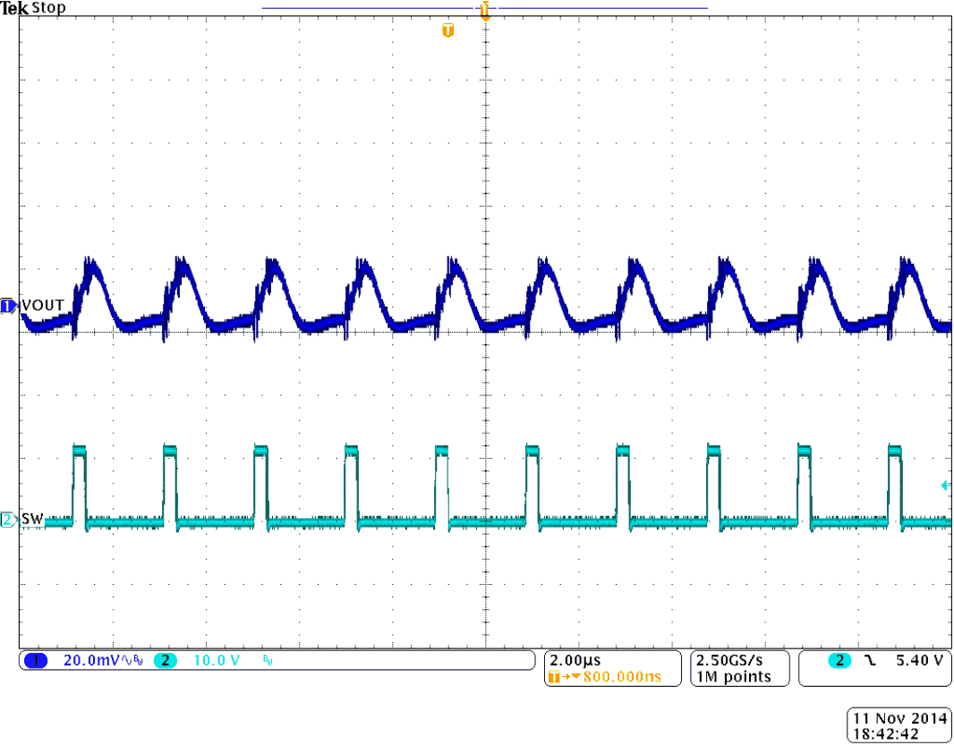
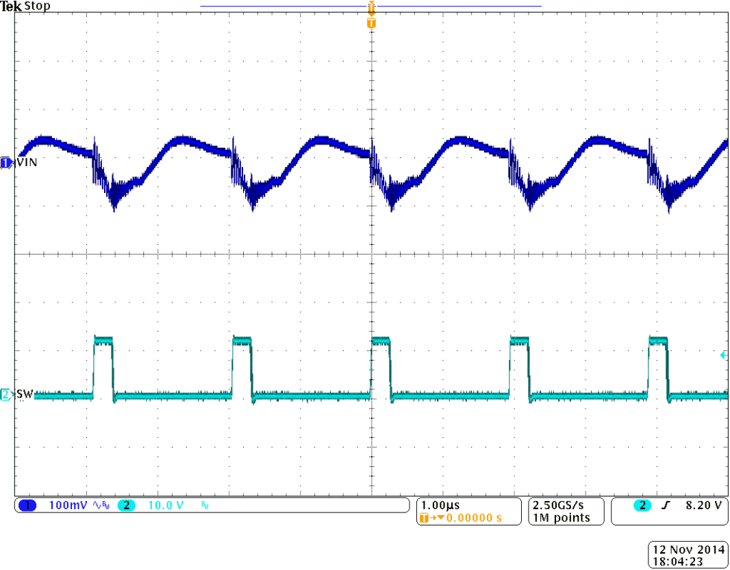
Another criterion for capacitor selection is the output ripple voltage. The output ripple is determined mainly by the capacitance and the ESR.
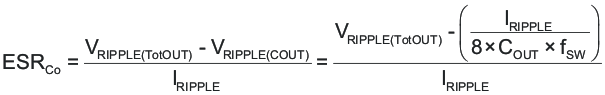
With 880-μF output capacitance, the ripple voltage at the capacitor is calculated to be 0.76 mV. In the specification, the output ripple voltage should be less than 30 mV, so based on Equation 24, the required maximum ESR is 11 mΩ. The selected capacitors can meet this requirement.
9.2.1.2.3 Step 3: Input Capacitor Selection
The input voltage ripple depends on the input capacitance and the ESR. The minimum capacitor and the maximum ESR can be estimated by:
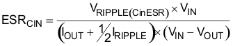
For this design, assume VRIPPLE(CIN) is 100 mV and VRIPPLE(CinESR) is 50 mV, so the calculated minimum capacitance is 43.6 μF and the maximum ESR is 2.7 mΩ. Choosing four 22-μF, 16-V, 2-mΩ ESR ceramic capacitors meets this requirement.
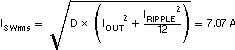
Another important consideration for the input capacitor is the RMS ripple current rating. The RMS current in the input capacitor is estimated by:

D is the duty cycle. The calculated RMS current is 6.6 A. Each selected ceramic capacitor has a RMS current rating of 4.3 A, so it is sufficient to reach this requirement.
9.2.1.2.4 Step 4: MOSFET Selection
The MOSFET selection determines the converter efficiency. In this design, the duty cycle is very small so that the high-side MOSFET is dominated with switching losses and the low-side MOSFET is dominated with conduction loss. To optimize the efficiency, choose smaller gate charge for the high-side MOSFET and smaller RDS(on) for the low-side MOSFET.
The RENESAS RJK0305 and RJK0301 are selected as the high-side and low-side MOSFETs respectively. To reduce the conduction loss, two RJK0301 components are used.
The power losses in the high-side MOSFET is calculated with the following equations:
The RMS current in the high side MOSFET is show in Equation 28.
The RDS(on) is 13 mΩ when the MOSFET gate voltage is 4.5 V.
The conduction loss is:

The switching loss is:
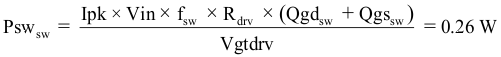
The calculated total loss in the high-side MOSFET is:

The power losses in the low-side SR MOSFET is calculated in the following equations:
The RMS current in the low-side MOSFET is shown in Equation 32.
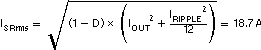
The RDS(on) is 4 mΩ when the MOSFET gate voltage is 4.5 V.
The total conduction loss in the two low-side MOSFETs is shown in Equation 33.
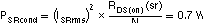
where
- N is the number of MOSFETs. Here, it is equal to 2.
The total power loss in the body diode is:

So the calculated total loss in the SR MOSFET is:

9.2.1.2.5 Step 5: Peripheral Component Design
9.2.1.2.5.1 Switching Frequency Setting (RT Pin 5)
In the design, a 62-kΩ resistor is selected. The actual switching frequency is 510 kHz.
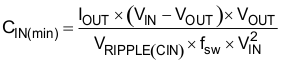
9.2.1.2.5.2 Output Voltage Setting (FB1 Pin 36)
Substitute R1 with 10 kΩ and then calculate RBIAS.
9.2.1.2.5.3 Current Sensing Network Design (CS1 Pin 31 and CSRT1 Pin 32)
For small pulse width, to avoid the sub-harmonics brought by the loop delay, a resistor divider is usually used to attenuate the current feedback information as described in the Inductor DCR Current Sense section.
Choosing C1 a value for 0.1-μF, and let R1 and R2 be equal, calculating R1 and R2 with Equation 38 and Equation 39. In this design, R1 and R2 are 10 kΩ.
A simplified equation to determine if the design produces sub-harmonics is shown in Equation 40.
In this design, a 1-μF capacitor is placed at the CSRT1 pin for the purpose of eliminating noise. It can be removed without degrading performance.
9.2.1.2.5.4 Overcurrent Protection (ILIM1 Pin 34)
The resistor selection equations in the CALCULATING OVERCURRENT PROTECTION LEVEL section are simplified to calculate the over current setting resistors. Set the DC over current rating at 30 A.
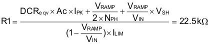
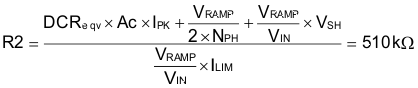
where
- AC is the gain transfer to comparator (typ 12.5)
- VRAMP is the ramp amplitude (typ 0.5 V)
- VSH is the VSHARE reference voltage (typ 1.8 V)
- ILIM is the current limit output current (typ 20 µA)
- NPH is 6 if VPHSEL = 1.6 V ±0.2 V, otherwise NPH = 8
9.2.1.2.5.5 VREG (Pin 21)
A 4.7-μF capacitor is connected to VREG pin to filter noise.
9.2.1.2.5.6 BP5 (Pin 8)
A 4.7-Ω and 1-μF capacitor is placed between VREG and BP5.
9.2.1.2.5.7 PHSEL (Pin 4)
For this dual output configuration, the PHSEL pin is directly tied to GND. The channel 1 and channel 2 has a 180° phase shift.
9.2.1.2.5.8 VSHARE (Pin 6)
A 1-μF capacitor is tied from VSHARE pin to GND.
9.2.1.2.5.9 PGOOD1 (Pin 30)
The PGOOD1 pin is tied to BP5 with a 10-kΩ resistor.
9.2.1.2.5.10 UVLO_CE1 (Pin 29)
It is connected to the input voltage with a resistor divider. The two resistors have the same value of 10-kΩ. When the input voltage is higher than 2 V, the chip is enabled.
9.2.1.2.5.11 Clkio (Pin 28)
CLKIO is floating as no clock synchronization required for dual output configuration.
9.2.1.2.5.12 BOOT1 and SW1 (Pin 27 and 25)
A bootstrap capacitor is connected between the BOOT1 and SW1 pin. The bootstrap capacitor depends on the total gate charge of the high side MOSFET and the amount of droop allowed on the bootstrap capacitor.
For this application, a 0.1-μF capacitor is selected.
9.2.1.2.5.13 TRK1 (Pin 33)
A 22-nF capacitor is tied to TRK1 pin to provide 1.28-ms of soft-start time.

9.2.1.2.5.14 DIFFO, VOUT, and GSNS (Pin 1, Pin 2, and Pin 3)
VOUT and GSNS are connected to the remote sensing output connector. DIFFO is connected to the feedback resistor divider. If the differential amplifier is not used, VOUT and GSNS are suggested to be grounded, and DIFFO is left open.
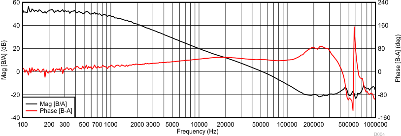
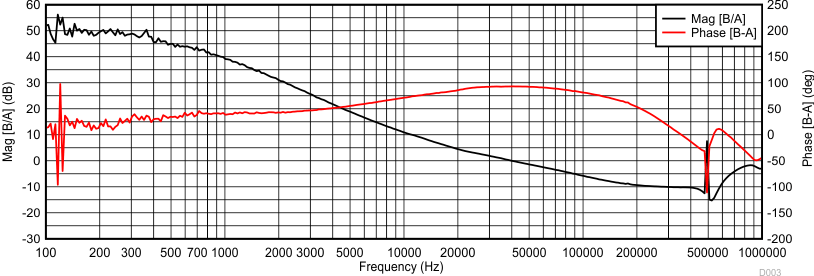
9.2.1.2.6 Feedback Compensator Design (COMP1 Pin 35)
Peak current mode control method is employed in the controller. A small signal model is developed from the COMP signal to the output.
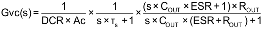
The time constant is defined by:
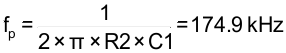
The low-frequency pole is calculated by:
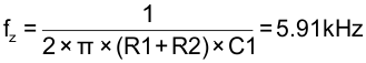
The ESR zero is calculated by:
In this design, a Type II compensator is employed to compensate the loop.
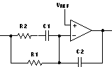 Figure 41. Type II Compensator
The compensator transfer function is:
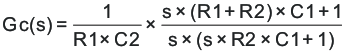
The loop gain transfer function is:

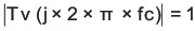
Assume the desired crossover frequency is 60 kHz, then set the compensator zero about 1/10 of the crossover frequency and the compensator pole equal to the ESR zero. The compensator gain is then calculated to achieve the desired bandwidth. In this design, the compensator gain, pole and zero are selected as following:
The compensator gain is solved as 400.
where
- C1 = 2.6 nF
- C2 = 250 pF
- R2 = 350 Ω
- Set R1 equal to 10-kΩ, and then calculate all the other components
In the real laboratory practice, the final components are selected as following to increase the phase margin and reduce PWM jitter.
- R1 = 10 kΩ
- C2 = 330 pF
- R2 = 50 Ω
- C1 = 2.2 nF
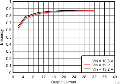
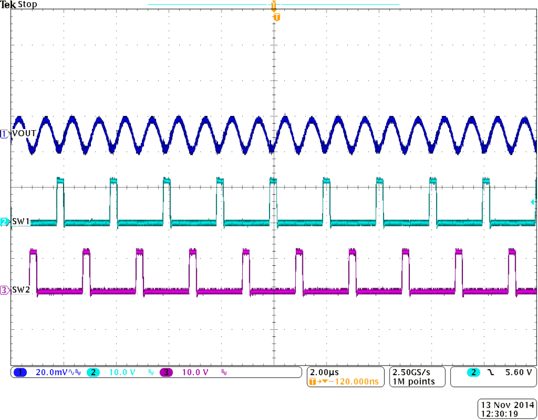
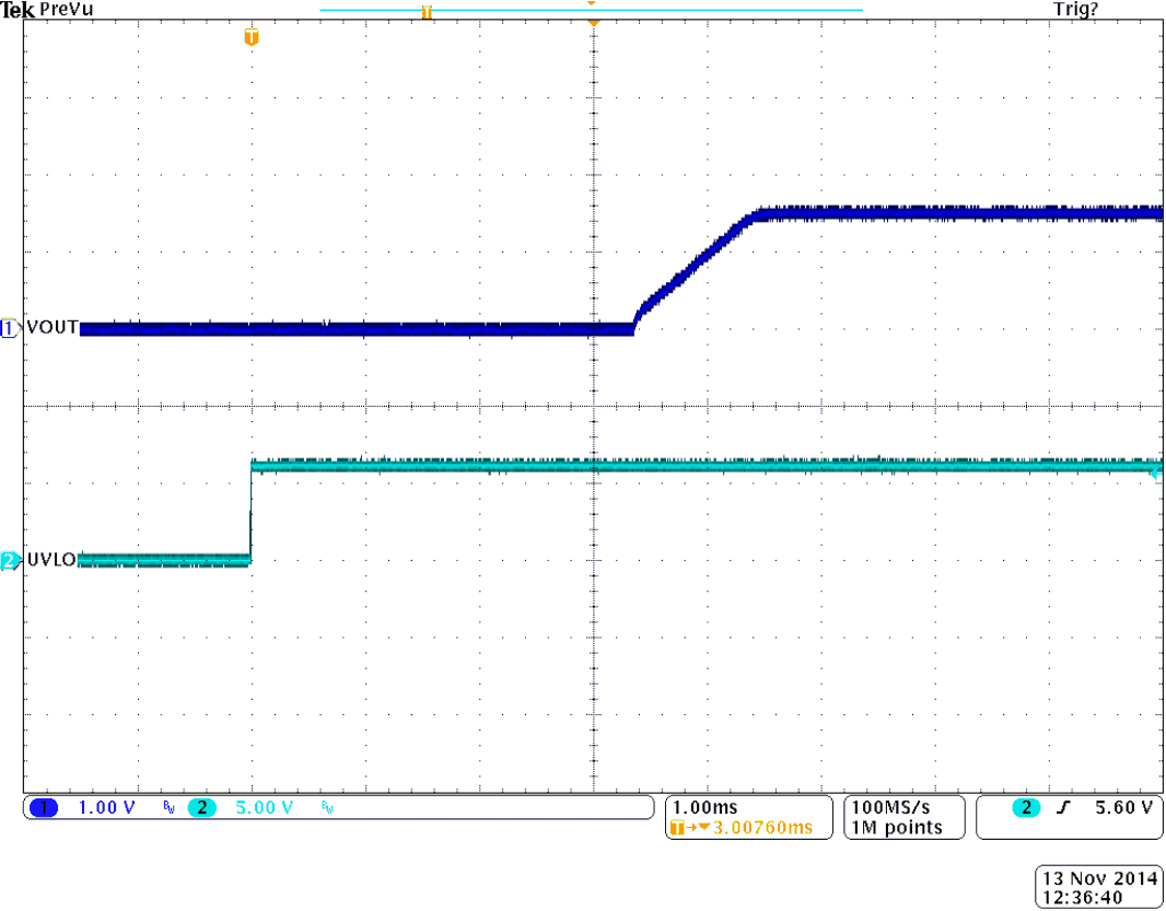
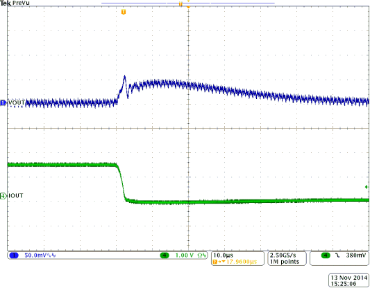
9.2.1.3 Application Curves
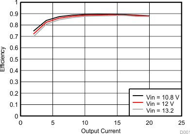
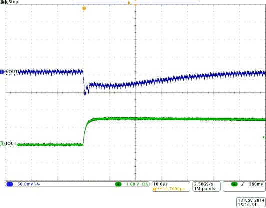
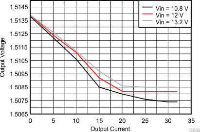
| VIN = 12 V | VOUT = 1.5 V | IOUT = 20A |
| VIN = 12 V | VOUT = 1.5 V | IOUT = 0A |
| VIN = 12 V | VOUT = 1.5 V |
| VIN = 12 V | VOUT = 1.5 V |
| VIN = 12 V | VOUT = 1.5 V | IOUT = 20A |
| VIN = 12 V | VOUT = 1.5 V | IOUT = 1A |
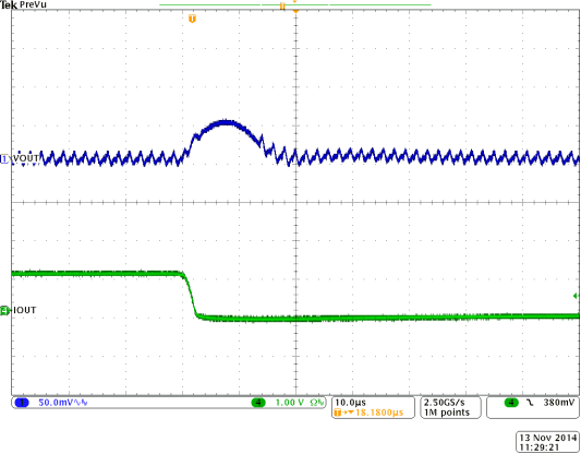
| VIN = 12 V | VOUT = 1.5 V |
| VIN = 12 V | VOUT = 1.5 V | IOUT = 20A |
9.2.2 Application 2: Two-Phase Single Output Configuration from 12 to 1.5 V DC-DC Converter Using a TPS40140
The following example illustrates the design process and component selection for a two-phase single output synchronous buck converter using TPS40140. The design goal parameters are given in Table 7. The inductor and MOSFET selection equations are quite similar to the dual output converter design, so they are not repeated here.
Figure 52 shows the schematic of the two phase single output converter design.
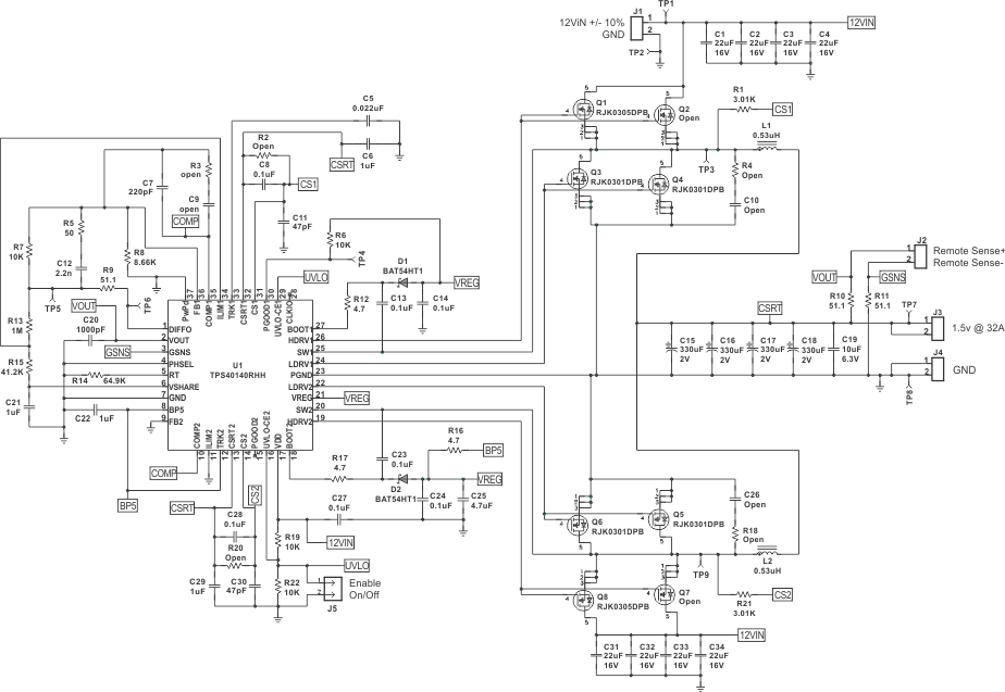 Figure 52. Two-Phase Single Output Converter Schematic
9.2.2.1 Design Requirements
Table 7. Design Goal Parameters
| PARAMETER | TEST CONDITION | MIN | TYP | MAX | UNIT | |
|---|---|---|---|---|---|---|
| VIN | Input voltage | 10.8 | 12 | 13.2 | V | |
| VIN(ripple) | Input ripple voltage | IOUT = 32 A | 0.15 | V | ||
| VOUT | Output voltage | 1.5 | V | |||
| Line regulation | 10.8 V ≤ VIN ≤ 13.2 V | 0.5% | ||||
| Load regulation | 0 V ≤ IOUT ≤ 32 A | 0.5% | ||||
| VP-P | Output ripple voltage | IOUT = 32 A | 30 | mV | ||
| ΔVOUT | Output voltage deviation during load transient | ΔIOUT = 15 A, VIN = 12 V | 50 | mV | ||
| IOUT | Output current | 10.8 V ≤ VIN ≤ 13.2 V | 0 | 32 | A | |
| η | Efficiency | IOUT = 32 A VIN = 12 V | 87% | |||
| fSW | Switching frequency | 500 | kHz | |||
9.2.2.2 Detailed Design Procedure
9.2.2.2.1 Step 1: Output Capacitor Selection
The output capacitor is typically selected by the output load transient response requirement. Equation 23 in the dual output design example is used. The inductor L in the equation is equal to the phase inductance divided by number of phases.
Based on a 15-A load transient with a maximum of 50 mV deviation, a minimum 795-μF output capacitor is required. In the design, four 330-μF, 2 V, SP capacitor are selected to meet this requirement. Each capacitor has an ESR of 6 mΩ.
Another criterion for capacitor selection is the output ripple voltage that is determined mainly by the capacitance and the ESR.
Due to the interleaving of channels, the total output ripple current is smaller than the ripple current from a single phase. The ripple cancellation factor is expressed in Equation 56.
where
- D is the duty cycle for a single phase
- NPH is the number of active phases, here it is equal to 2
- m = floor (NPH × D) is the maximum integer that does not exceed the (NPH × D), here m is 0
The output ripple current is then calculated in Equation 57. The maximum output ripple current is 4.3 A with maximum input voltage.

With 1.32 mF output capacitance, the ripple voltage at the capacitor is calculated to be 0.82 mV. In the specification, the output ripple voltage should be less than 30 mV, so based on Equation 24, the required maximum ESR is 6.7 mΩ. The selected capacitors can meet this requirement.
9.2.2.2.2 Step 2: Input Capacitor Selection
The input voltage ripple depends on the input capacitance and the ESR. The minimum capacitor and the maximum ESR can be estimated by Equation 25 and Equation 26 in the dual output design example. The phase current should be used in the calculation.
For this design, VRIPPLE(CIN) assume is 100mV and VRIPPLE(CinESR) is 50 mV, so the calculated minimum capacitance is 40 μF and the maximum ESR is 2.7 mΩ. Choosing four 22-μF, 16-V, 2-mΩ ESR ceramic capacitors meet this requirement.
Another important consideration for the input capacitor is the RMS ripple current rating. Due to the interleaving of multi-phase, the input RMS current is reduced. The input ripple current RMS value over load current is calculated in Equation 58.

where
- D is the duty cycle for a single phase
- NPH is the number of active phases, here it is equal to 2
- m = floor (NPH × D) is the maximum integer that does not exceed the (NPH × D), here m is 0
The input ripple RMS current is calculated in Equation 59. In this design, the maximum IIN_NORM is calculated to be 0.225 with the minimum input voltage, and the maximum input ripple RMS current is 7.2 A. Each selected ceramic capacitor has a RMS current rating of 4.3 A, therefore, sufficient to reach this requirement.
9.2.2.2.3 Step 3: Peripheral Component Design
9.2.2.2.3.1 Switching Frequency Setting (Rt Pin 5)

where
- ƒsw represents the phase switching frequency
In the design, a 64.9-kΩ resistor is selected. The actual switching frequency is 490 kHz.
9.2.2.2.3.2 COMP1 and COMP2 (Pin 35 and Pin 10)
COMP1 is connected to the compensator network. The selection of compensation components is similar to the dual output design example.
COMP2 is directly tied to COMP1.
9.2.2.2.3.3 TRK1 and TRK2 (Pin 33 and Pin 12)
A soft start capacitor is connected between TRK1 and GND. TRK2 is directly tied to BP5 to set this channel as a slave
9.2.2.2.3.4 ILIM1 and ILIM2 (Pin 34 and Pin 11)
ILIM1 is connected to the resistor network that has the same design as the dual output example. The peak current in Equation 42 and Equation 43 is the peak current of each phase.
ILIM2 is connected to GND.
9.2.2.2.3.5 FB1 and FB2 (Pin 36 and Pin 9)
FB1 is tied to the feedback network. FB2 is connected to GND.
9.2.2.2.3.6 PHSEL (Pin 4)
For this two phase configuration, the PHSEL pin is directly tied to GND.
9.2.2.2.3.7 PGOOD1 and PGOOD2 (Pin 30 and Pin 15)
Both of PGOOD1 and PGOOD2 are tied to BP5 with a 10-kΩ resistor.
9.2.2.2.3.8 CLKIO (Pin 28)
CLKIO is open as no clock synchronization required for two phase configuration.
9.2.2.2.3.9 DIFFO, VOUT, and GSNS (Pin 1, Pin 2, and Pin 3)
VOUT and GSNS should be connected to the remote sensing output connector. DIFFO is connected to the feedback resistor divider. If the differential amplifier is not used, VOUT and GSNS are suggested to be grounded, and DIFFO is left open.
9.2.3 Application Curves
| VIN = 12 V | VOUT = 1.5 V | IOUT = 32A |
| VIN = 12 V | VOUT = 1.5 V | IOUT = 0A |
| VIN = 12 V | VOUT = 1.5 V |
| VIN = 12 V | VOUT = 1.5 V |
| VIN = 12 V | VOUT = 1.5 V | IOUT = 32A |
| VIN = 12 V | VOUT = 1.5 V | IOUT = 1A |
| VIN = 12 V | VOUT = 1.5 V |
| VIN = 12 V | VOUT = 1.5 V | IOUT = 32A |
9.3 System Example
9.3.1 Four-Phase Single Output Configuration from 12 to 1.8 V DC-DC Converter Using Two TPS40140
The following example illustrates the design process and component selection for a 4-phase single output synchronous buck converter using two TPS40140.
Here, two modules are designed. One is a master module. The other one is a slave module. Each module contains two phases and each phase handle 5 A. The two modules are stacked together to form a 4-phase converter. More slave modules can be stacked to this converter to get the desired phases. The modules are plugged into a mother board.
Figure 63, Figure 64, and Figure 65 shows the schematics of the four phase converter design.
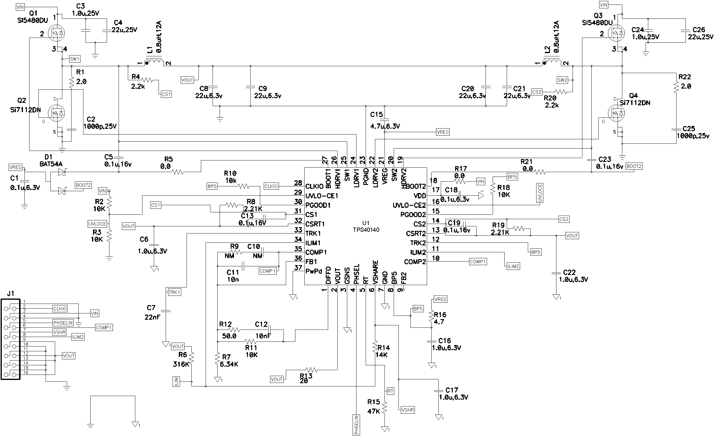 Figure 63. Master Module Schematic
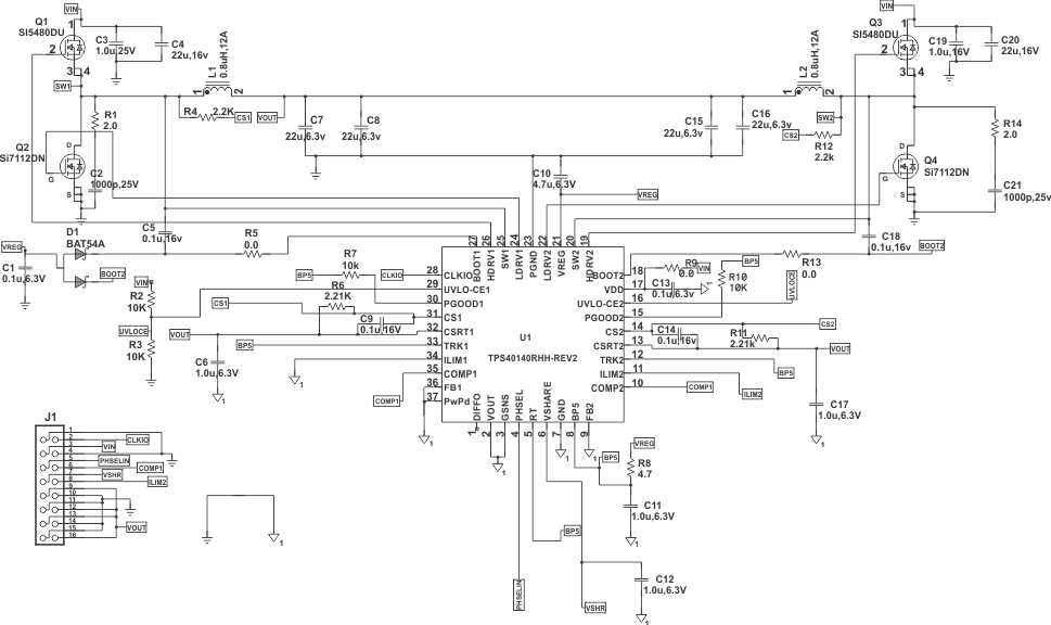 Figure 64. Slave Module Schematic
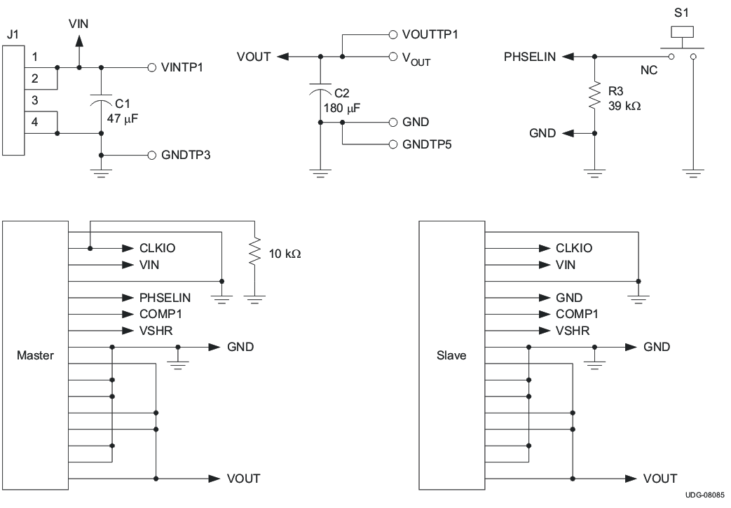 Figure 65. Motherboard Schematic
The design goal parameters are given in Table 8.
Table 8. Design Goal Parameters
| PARAMETER | TEST CONDITIONS | MIN | TYP | MAX | UNIT | |
|---|---|---|---|---|---|---|
| VIN | Input Voltage | 10.8 | 12 | 13.2 | V | |
| VOUT | Output voltage | 1.8 | V | |||
| VRIPPLE | Output ripple | IO = 20 A | 20 | mV | ||
| IPH | Phase current | 5 | A | |||
| fsw | Switching frequency | 650 | kHz | |||
| NPH | Phase number | 4 | ||||
9.3.1.1 Step 1: Output Capacitor Selection
The output capacitor is typically selected by the output load transient response requirement. Equation 23 in the dual output design example is used. Also, as mentioned in the two phase design example, the inductor is equivalent to  . Based on a 10-A load transient with a maximum of 30 mV deviation, a minimum 370-μF output capacitor is required. In the design, one 180 μF, 6.3 V, SP capacitor is placed on the mother board. Four 22-μF, 6,3-V ceramic capacitors are placed on each module. The total output capacitance is 356 μF.
The output ripple current cancellation factor is calculated to be 0.526 with maximum input voltage based on Equation 56.
So the maximum output ripple current is calculated by:

With 356-μF output capacitance, the ripple voltage at the capacitor is calculated to be 0.85 mV. In the specification, the output ripple voltage should be less than 20 mV, so based on Equation 24, the required maximum ESR is 12 mΩ. The selected capacitors can reach this requirement.
9.3.1.2 Step 2: Input Capacitor Selection
The input voltage ripple depends on the input capacitance and the ESR. The minimum capacitor and the maximum ESR can be estimated by Equation 25 and Equation 26 in the dual output design example.
For this design, assume VRIPPLE(CIN) is 50 mV and VRIPPLE(CinEST) is 30 mV, also each phase inductor ripple current is 50%, so the calculated minimum capacitance is 23-μF and the maximum ESR is 4.6 mΩ. In this case, one 33-μF 6.3-V SP-capacitor is placed on the mother board and each module has two 22-μF, 6.3-V ceramic capacitors.
The maximum input ripple RMS current is calculated to be 2.57 A with the maximum input voltage based on Equation 58. The selected capacitors are sufficient to meet this requirement.
9.3.1.3 Step 3: Peripheral Component Design
9.3.1.3.1 Master Module
9.3.1.3.1.1 Rt (Pin 5)
It is connected to GND with a resistor that sets the switching frequency.

Here, ƒsw represents the phase switching frequency. In the design, a 47-kΩ resistor is selected. The actual switching frequency is 650 kHz.
9.3.1.3.1.2 COMP1 and COMP2 (Pin 35 and Pin 10)
COMP1 is connected to the compensator network.
COMP2 is directly tied to COMP1.
9.3.1.3.1.3 TRK1 and TRK2 (Pin 33 and Pin 12)
A soft start capacitor is connected between TRK1 and GND. TRK2 is directly tied to BP5 to set this channel as a salve.
9.3.1.3.1.4 ILIM1 and ILIM2 (Pin 34 and Pin 11)
ILIM1 is connected to the resistor network that has the same design as the dual output example. The peak current in Equation 42 and Equation 43 is the peak current of each phase.
ILIM2 is grounded.
9.3.1.3.1.5 FB1 and FB2 (Pin 36 and Pin 9)
FB1 is tied to the feedback network. FB2 is connected to GND.
9.3.1.3.1.6 PHSEL (Pin 4)
For this four phase configuration, the PHSEL pin is tied to GND with a 39-kΩ resistor.
9.3.1.3.1.7 PGOOD1 and PGOOD2 (Pin 30 and Pin 15)
Both of PGOOD1 and PGOOD2 are tied to BP5 with a 10-kΩ resistor.
9.3.1.3.1.8 CLKIO (Pin 28)
CLKIO is connected to the same pin in the salve module.
9.3.1.3.2 Slave Module:
9.3.1.3.2.1 RT (Pin 5)
It is connected to BP5. The slave module receives the clock from the master module.
9.3.1.3.2.2 COMP1 and COMP2 (Pin 35 and Pin 10)
Both of COMP1 and COMP2 are directly tied together to COMP1 or COMP2 in the master module.
9.3.1.3.2.3 TRK1 and TRK2 (Pin 33 and Pin 12)
Both TRK1 and TRK2 are directly tied to BP5.
9.3.1.3.2.4 ILIM1 and ILIM2 ( Pin 34 and Pin 11)
Both ILIM1 and ILIM2 are grounded.
9.3.1.3.2.5 FB1 and FB2 (Pin 36 and Pin 9)
Both FB1 and FB2 are connected to GND.
9.3.1.3.2.6 PHSEL (Pin 4)
The PHSEL pin is directly tied to GND.
9.3.1.3.2.7 PGOOD1 and PGOOD2 (Pin 30 and Pin 15)
Both of PGOOD1 and PGOOD2 are tied to BP5 with a 10-kΩ resistor.
9.3.1.3.2.8 CLKIO (Pin 28)
CLKIO is connected to the master module CLKIO.