SLUS660I September 2005 – January 2015 TPS40140
PRODUCTION DATA.
- 1 Features
- 2 Applications
- 3 Description
- 4 Revision History
- 5 Device Comparison Table
- 6 Pin Configuration and Functions
- 7 Specifications
- 8 Detailed Description
-
9 Application and Implementation
- 9.1
Application Information
- 9.1.1 Synchronizing a Single Controller to an External Clock
- 9.1.2 Split Input Voltage Operation
- 9.1.3 Configuring Single and Multiple ICs
- 9.1.4 Digital Clock Synchronization
- 9.1.5 Typical Start-Up Sequence
- 9.1.6 Track (Soft-Start Without PreBiased Output)
- 9.1.7 Soft-Start With PreBiased Outputs
- 9.1.8 Track Function in Configuring a Slave Channel
- 9.1.9 Differential Amplifier, U9
- 9.1.10 Setting the Output Voltage
- 9.1.11 Programmable Input UVLO Protection
- 9.1.12 CLKFLT, CLKIO Pin Fault
- 9.1.13 PHSEL Pin Fault
- 9.1.14 Overtemperature
- 9.1.15 Fault Masking Operation
- 9.1.16 Setting the Switching Frequency
- 9.1.17 Current Sense
- 9.1.18 Current Sensing and Balancing
- 9.1.19 Overcurrent Detection and Hiccup Mode
- 9.1.20 Calculating Overcurrent Protection Level
- 9.1.21 Design Examples Information
- 9.2
Typical Application
- 9.2.1
Application 1: Dual-Output Configuration from 12 to 3.3 V and 1.5 V DC-DC Converter Using a TPS40140
- 9.2.1.1 Design Requirements
- 9.2.1.2
Detailed Design Procedure
- 9.2.1.2.1 Step 1: Inductor Selection
- 9.2.1.2.2 Step 2: Output Capacitor Selection
- 9.2.1.2.3 Step 3: Input Capacitor Selection
- 9.2.1.2.4 Step 4: MOSFET Selection
- 9.2.1.2.5
Step 5: Peripheral Component Design
- 9.2.1.2.5.1 Switching Frequency Setting (RT Pin 5)
- 9.2.1.2.5.2 Output Voltage Setting (FB1 Pin 36)
- 9.2.1.2.5.3 Current Sensing Network Design (CS1 Pin 31 and CSRT1 Pin 32)
- 9.2.1.2.5.4 Overcurrent Protection (ILIM1 Pin 34)
- 9.2.1.2.5.5 VREG (Pin 21)
- 9.2.1.2.5.6 BP5 (Pin 8)
- 9.2.1.2.5.7 PHSEL (Pin 4)
- 9.2.1.2.5.8 VSHARE (Pin 6)
- 9.2.1.2.5.9 PGOOD1 (Pin 30)
- 9.2.1.2.5.10 UVLO_CE1 (Pin 29)
- 9.2.1.2.5.11 Clkio (Pin 28)
- 9.2.1.2.5.12 BOOT1 and SW1 (Pin 27 and 25)
- 9.2.1.2.5.13 TRK1 (Pin 33)
- 9.2.1.2.5.14 DIFFO, VOUT, and GSNS (Pin 1, Pin 2, and Pin 3)
- 9.2.1.2.6 Feedback Compensator Design (COMP1 Pin 35)
- 9.2.1.3 Application Curves
- 9.2.2
Application 2: Two-Phase Single Output Configuration from 12 to 1.5 V DC-DC Converter Using a TPS40140
- 9.2.2.1 Design Requirements
- 9.2.2.2
Detailed Design Procedure
- 9.2.2.2.1 Step 1: Output Capacitor Selection
- 9.2.2.2.2 Step 2: Input Capacitor Selection
- 9.2.2.2.3
Step 3: Peripheral Component Design
- 9.2.2.2.3.1 Switching Frequency Setting (Rt Pin 5)
- 9.2.2.2.3.2 COMP1 and COMP2 (Pin 35 and Pin 10)
- 9.2.2.2.3.3 TRK1 and TRK2 (Pin 33 and Pin 12)
- 9.2.2.2.3.4 ILIM1 and ILIM2 (Pin 34 and Pin 11)
- 9.2.2.2.3.5 FB1 and FB2 (Pin 36 and Pin 9)
- 9.2.2.2.3.6 PHSEL (Pin 4)
- 9.2.2.2.3.7 PGOOD1 and PGOOD2 (Pin 30 and Pin 15)
- 9.2.2.2.3.8 CLKIO (Pin 28)
- 9.2.2.2.3.9 DIFFO, VOUT, and GSNS (Pin 1, Pin 2, and Pin 3)
- 9.2.3 Application Curves
- 9.2.1
Application 1: Dual-Output Configuration from 12 to 3.3 V and 1.5 V DC-DC Converter Using a TPS40140
- 9.3
System Example
- 9.3.1
Four-Phase Single Output Configuration from 12 to 1.8 V DC-DC Converter Using Two TPS40140
- 9.3.1.1 Step 1: Output Capacitor Selection
- 9.3.1.2 Step 2: Input Capacitor Selection
- 9.3.1.3
Step 3: Peripheral Component Design
- 9.3.1.3.1
Master Module
- 9.3.1.3.1.1 Rt (Pin 5)
- 9.3.1.3.1.2 COMP1 and COMP2 (Pin 35 and Pin 10)
- 9.3.1.3.1.3 TRK1 and TRK2 (Pin 33 and Pin 12)
- 9.3.1.3.1.4 ILIM1 and ILIM2 (Pin 34 and Pin 11)
- 9.3.1.3.1.5 FB1 and FB2 (Pin 36 and Pin 9)
- 9.3.1.3.1.6 PHSEL (Pin 4)
- 9.3.1.3.1.7 PGOOD1 and PGOOD2 (Pin 30 and Pin 15)
- 9.3.1.3.1.8 CLKIO (Pin 28)
- 9.3.1.3.2
Slave Module:
- 9.3.1.3.2.1 RT (Pin 5)
- 9.3.1.3.2.2 COMP1 and COMP2 (Pin 35 and Pin 10)
- 9.3.1.3.2.3 TRK1 and TRK2 (Pin 33 and Pin 12)
- 9.3.1.3.2.4 ILIM1 and ILIM2 ( Pin 34 and Pin 11)
- 9.3.1.3.2.5 FB1 and FB2 (Pin 36 and Pin 9)
- 9.3.1.3.2.6 PHSEL (Pin 4)
- 9.3.1.3.2.7 PGOOD1 and PGOOD2 (Pin 30 and Pin 15)
- 9.3.1.3.2.8 CLKIO (Pin 28)
- 9.3.1.3.1
Master Module
- 9.3.1
Four-Phase Single Output Configuration from 12 to 1.8 V DC-DC Converter Using Two TPS40140
- 9.1
Application Information
- 10Power Supply Recommendations
- 11Layout
- 12Device and Documentation Support
- 13Mechanical, Packaging, and Orderable Information
6 Pin Configuration and Functions
RHH PACKAGE
VQFN 36-PINS
(TOP VIEW)
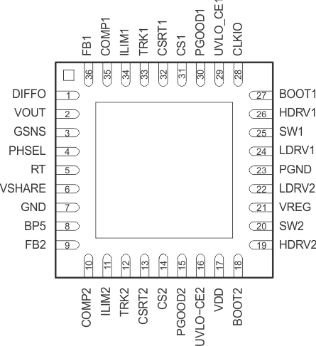
The thermal pad is an electrical ground connection.
Pin Functions
| PIN(1) | I/O | DESCRIPTION | |
|---|---|---|---|
| NAME | NO. | ||
| BOOT1 | 27 | I | BOOT1 provides a bootstrapped supply for the high side FET driver for PWM1, enabling the gate of the high side FET to be driven above the input supply rail. Connect a capacitor from BOOT1 to SW1 pin and a Schottky diode from this pin to VREG. |
| BOOT2 | 18 | I | BOOT2 provides a bootstrapped supply for the high side FET driver for PWM2, enabling the gate of the high side FET to be driven above the input supply rail. Connect a capacitor from BOOT2 to SW2 pin and a Schottky diode from this pin to VREG. |
| BP5 | 8 | I | Filtered input from the VREG pin. A 10-Ω resistor should be connected between VREG and BP5 and a 1.0-μF ceramic capacitor should be connected from BP5 to ground. |
| CLKIO | 28 | O | Digital clock signal for synchronizing slave controllers to the master CLKIO frequency and is either 6 or 8 times the PWM switching frequency. |
| COMP1 | 35 | O | Output of the error amplifier, CH1. The voltage at this pin determines the duty cycle for the PWM1. |
| COMP2 | 10 | O | Output of the error amplifier, CH2. The voltage at this pin determines the duty cycle for the PWM2. |
| CS1 | 31 | I | These pins are used to sense the CH1 phase current. Inductor current can be sensed with an external current sense resistor or by using an external R-C circuit and the inductor’s DC resistance. The traces for these signals must be connected directly at the current sense element. |
| CS2 | 14 | I | These pins are used to sense the CH2 phase current. Inductor current can be sensed with an external current sense resistor or by using an external R-C circuit and the inductor’s DC resistance. The traces for these signals must be connected directly at the current sense element. |
| DIFFO | 1 | O | Output of the differential amplifier. The output voltage of the differential amplifier is limited to 5.8 V. For remote sensing, the voltage at this pin represents the true output voltage without I × R drops that result from high current in the PCB traces. The VOUT and GSNS pins must be connected directly at the point of load where regulation is required. See Layout Guidelines for more information. |
| CSRT1 | 32 | I | Return point of CH1 current sense voltage. The trace for this signal must be connected directly at the current sense element. |
| CSRT2 | 13 | I | Return point of CH1 current sense voltage. The trace for this signal must be connected directly at the current sense element. |
| FB1 | 36 | I | Inverting input of the error amplifier for CH1. In closed loop operation, the voltage at this pin is nominally 700 mV. This pin is also monitored for PGOOD1 and undervoltage on CH1. |
| FB2 | 9 | I | Inverting input of the error amplifier for CH2. In closed loop operation, the voltage at this pin is nominally 700 mV. This pin is also monitored for PGOOD2 and undervoltage on CH2. |
| GND | 7 | — | Low noise ground connection to the device. |
| GSNS | 3 | I | Inverting input of the differential amplifier. This pin should be connected to ground at the load. If the differential amplifier is not used, tie this pin to GND or leave open. |
| HDRV1 | 26 | O | Gate drive output for the high-side N-channel MOSFET switch for CH1. Output is referenced to SW1 and is bootstrapped for enhancement of the high side switch. |
| HRDV2 | 19 | O | Gate drive output for the high-side N-channel MOSFET switch for CH2. Output is referenced to SW2 and is bootstrapped for enhancement of the high side switch. |
| ILIM1 | 34 | I | Used to set the cycle-by-cycle current limit threshold for CH1. If the ILIM1 threshold is reached, the PWM pulse is terminated and the converter delivers limited current to the output. |
| ILIM2 | 11 | I | Used to set the cycle-by-cycle current limit threshold for CH2. If the ILIM2 threshold is reached, the PWM pulse is terminated and the converter delivers limited current to the output. |
| LRDV1 | 24 | O | Gate drive output for the low-side synchronous rectifier (SR) N-channel MOSFET for CH1. |
| LRDV2 | 22 | O | Gate drive output for the low-side synchronous rectifier (SR) N-channel MOSFET for CH2. |
| PGOOD1 | 30 | O | Power good indicators for CH1 output voltage. This open-drain output connects to a voltage via an external resistor |
| PGOOD2 | 15 | O | Power good indicators for CH2 output voltage. This open-drain output connects to a voltage via an external resistor |
| PGND | 23 | — | Power ground reference for the controller lower gate drivers. There should be a high current return path from the sources of the lower MOSFETs to this pin. |
| PHSEL | 4 | O | A 20μA current flows from this pin. In a single controller design, this pin should be grounded. In a multi controller configuration, a 39- kΩ resistor string sets the voltage on this pin determines the proper phasing for the slaves. See the section on Clock Master, PHSEL, and CLKIO Configurations. |
| RT | 5 | I | Connecting a resistor from this pin to ground sets the oscillator frequency. |
| SW1 | 25 | I | Connect to the switched node on converter CH1. It is the return for the CH 1 upper gate driver. There should be a high current return path from the source of the upper MOSFET to this pin. This pin is also used by the adaptive gate drive circuits to minimize the dead time between upper and lower MOSFET conduction. |
| SW2 | 20 | I | Connect to the switched node on converter CH2. It is the return for the CH 2 upper gate driver. There should be a high current return path from the source of the upper MOSFET to this pin. This pin is also used by the adaptive gate drive circuits to minimize the dead time between upper and lower MOSFET conduction. |
| TRK1 | 33 | I | This is an input to the non-inverting input of the error amplifier CH1. This pin is normally connected to the soft-start capacitor or to another voltage that is tracked. |
| TRK2 | 12 | I | This is an input to the non-inverting input of the error amplifier CH2. This pin is normally connected to the soft-start capacitor or to another voltage that is tracked. |
| UVLO_CE1 | 29 | I | A voltage divider from VIN to this pin determines the input voltage that CH1 starts. When the voltage is between 0.5 and 1.5 V the VREG regulator is enabled . When the voltage is 2.1 V or above CH1 soft start is allowed to begin. |
| UVLO_CE2 | 16 | I | A voltage divider from VIN to this pin determines the input voltage that CH2 starts. When the voltage is between 0.5 and 1.5 V the VREG regulator is enabled . When the voltage is 2.1 V or above CH2 soft start is allowed to begin. |
| VDD | 17 | I | Power input for the controller 5V regulator and differential amplifier. A 1.0-μF ceramic capacitor should be connected from this pin to ground. |
| VOUT | 2 | I | Non-inverting input of the differential amplifier. This pin should be connected to the output of the converter close to the load point. If the differential amplifier is not used, leave this pin open. |
| VREG | 21 | O | The output of the internal 5-V regulator. A 4.7-μF ceramic capacitor should be connected from this pin to PGND. |
| VSHARE | 6 | O | The 1.8-V reference output |
(1) It is often necessary to refer to a pin or pins that are used in CH1 and/or CH2. The shortcut nomenclature used is the pin name with a lower case 'x' to mean either or both channels. For example, TRKx refers to TRK1 and/or TRK2.