SLUS659G FEBRUARY 2006 – November 2014 TPS40200
PRODUCTION DATA.
- 1 Features
- 2 Applications
- 3 Description
- 4 Revision History
- 5 Pin Configuration and Functions
- 6 Specifications
- 7 Detailed Description
-
8 Application and Implementation
- 8.1 Application Information
- 8.2
Typical Application
- 8.2.1
Buck Regulator, 8 V to 12 V Input, 3.3 V to 5.0 V at 2.5-A Output
- 8.2.1.1 Design Requirements
- 8.2.1.2
Detailed Design Procedure
- 8.2.1.2.1 FET Selection Criteria
- 8.2.1.2.2 Rectifier Selection Criteria
- 8.2.1.2.3 Inductor Selection Criteria
- 8.2.1.2.4 Output Capacitance
- 8.2.1.2.5 Switching Frequency
- 8.2.1.2.6 Calculating the Overcurrent Threshold Level
- 8.2.1.2.7 Soft-Start Capacitor
- 8.2.1.2.8 Frequency Compensation
- 8.2.1.2.9 Printed Circuit Board Plots
- 8.2.1.3 Application Curves
- 8.2.2 18 V - 50 V Input, 16 V at 1-A Output
- 8.2.3 Wide Input Voltage Led Constant Current Driver
- 8.2.1
Buck Regulator, 8 V to 12 V Input, 3.3 V to 5.0 V at 2.5-A Output
- 9 Power Supply Recommendations
- 10Layout
- 11Device and Documentation Support
- 12Mechanical, Packaging, and Orderable Information
パッケージ・オプション
デバイスごとのパッケージ図は、PDF版データシートをご参照ください。
メカニカル・データ(パッケージ|ピン)
- D|8
- DRB|8
サーマルパッド・メカニカル・データ
- DRB|8
発注情報
7 Detailed Description
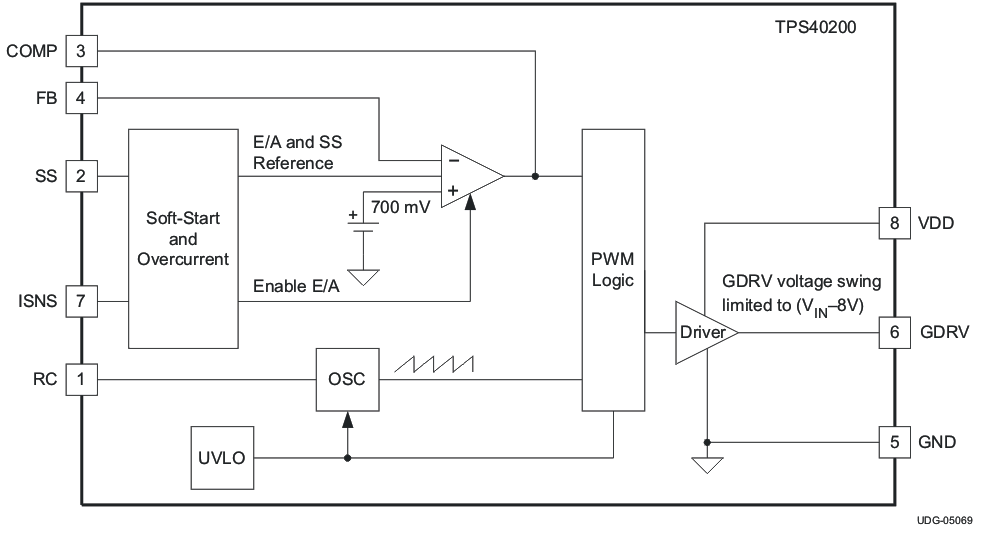
7.1 Overview
The TPS40200 is a non-synchronous controller with a built in 200-mA driver designed to drive high speed P-channel FETs up to 500 kHz. Small size combined with complete functionality makes the part both versatile and easy to use.
The controller uses a low-value current-sensing resistor in series with the input voltage and the power FETs source connection to detect switching current. When the voltage drop across this resistor exceeds 100 mV, the part enters an hiccup fault mode at about 2% of the operating frequency.
The device uses voltage feedback to an error amplifier that is biased by a precision 700-mV reference. Feed-forward compensation from the input keeps the PWM gain constant over the full input voltage range, eliminating the need to change frequency compensation for different input voltages.
The TPS40200 also incorporates a soft-start feature where the output follows a slowly rising soft-start voltage, preventing output-voltage overshoot.
7.2 Functional Block Diagram
7.3 Feature Description
7.3.1 MOSFET Gate Drive
The output driver sinking current is approximately 200 mA and is designed to drive P-channel power FETs. When the driver pulls the gate charge of the FET it is controlling to 8 V, the drive current folds back to a low level so that high-power dissipation only occurs during the turn-on period of the FET. This feature is particularly valuable when turning on a FET at high input voltages where leaving the gate drive current on would otherwise cause unacceptable power dissipation.
7.3.2 Undervoltage Lockout Protection
Undervoltage lockout (UVLO) protection ensures proper startup of the device only when the input voltage has exceeded minimum operating voltage. Undervoltage protection incorporates hysteresis which eliminates hiccup starting in cases where input supply impedance is high.
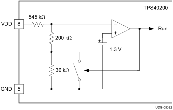 Figure 23. Undervoltage Lockout
Undervoltage protection ensures proper startup of the device only when the input voltage has exceeded minimum operating voltage. The UVLO level is measured at the VDD pin with respect to GND. Startup voltage is typically 4.3 V with approximately 200 mV of hysteresis. The device shuts off at a nominal 4.1 V. As shown in Figure 23, when the input VDD voltage rises to 4.3 V , the 1.3-V comparator’s threshold voltage is exceeded and a RUN signal occurs. Feedback from the output closes the switch, and shunts the 200-kΩ resistor so that an approximately 200 mV lower voltage, or 4.1 V, is required before the part shuts down.
7.3.3 Selecting the Operating Frequency
The operating frequency of the controller is determined by an external resistor RRC that is connected from the RC pin to VDD and a capacitor attached from the RC pin to ground. This connection and the two oscillator comparators inside the device, are shown in Figure 24. The oscillator frequency can be calculated in Equation 1.
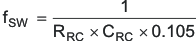
where
fSW is the clock frequency
RRC is the timing resistor value in Ω
CRC is the timing capacitor value in F
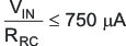
RRC must be kept large enough that the current through it does not exceed 750 μA when the internal switch (shown in Figure 24) is discharging the timing capacitor. This condition may be expressed by Equation 2.
7.3.4 Synchronizing the Oscillator
Figure 24 shows the functional diagram of the oscillator. When synchronizing the oscillator to an external clock, the RC pin must be pulled below 150 mV for 20 ns or more. The external clock frequency must be higher than the free running frequency of the converter as well. When synchronizing the controller, if the RC pin is held low for an excessive amount of time, erratic operation may occur. The maximum amount of time that the RC pin should be held low is 50% of a nominal output pulse, or 10% of the period of the synchronization frequency whichever is less.
Under circumstances where the input voltage is high and the duty cycle is less than 50%, a Schottky diode connected from the RC pin to an external clock may be used to synchronize the oscillator. The cathode of the diode is connected to the RC pin. The trip point of the oscillator is set by an internal voltage divider to be 1/10 of the input voltage. The clock signal must have an amplitude higher than this trip point. When the clock goes low, it allows the reset current to restart the RC ramp, synchronizing the oscillator to the external clock. This provides a simple, single-component method for clock synchronization.
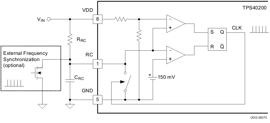 Figure 24. Oscillator Functional Diagram
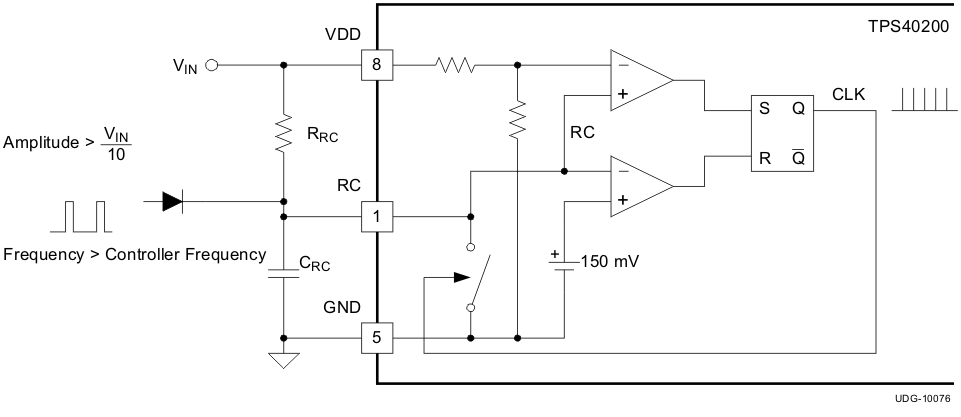 Figure 25. Diode-Connected Synchronization
7.3.5 Current Limit Resistor Selection
As shown in Figure 28, a resistor in series with the power MOSFET sets the overcurrent protection level. Use a low-inductance resistor to avoid ringing signals and nuisance tripping. When the FET is on and the controller senses 100 mV or more drop from the VDD pin to the ISNS pin, an overcurrent condition is declared. When this happens, the FET is turned off, and as shown in Figure 26, the soft-start capacitor is discharged. When the soft-start capacitor reaches a level below 150 mV, the converter clears the overcurrent condition flag and attempts to restart. If the condition that caused the overcurrent event to occur is still present on the output of the converter (see Figure 27), another overcurrent condition is declared and the process repeats indefinitely. Figure 27 shows the soft-start capacitor voltage during an extended output fault condition. The overall duty cycle of current conduction during a persistent fault is approximately 2%.
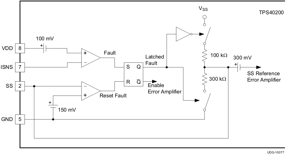 Figure 26. Current Limit Reset
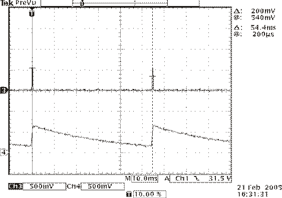 Figure 27. Typical Soft-Start Capacitor and VOUT During Overcurrent
If necessary, a small RC filter can be added to the current sensing network to reduce nuisance tripping due to noise pickup. This filter can also be used to trim the overcurrent trip point to a higher level with the addition of a single resistor. See Figure 28. The nominal overcurrent trip point using the circuit of Figure 28 is described in Equation 3.
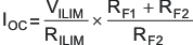
Where
IOC is the overcurrent trip point, peak current in the inductor
VILIM is the overcurrent threshold voltage for the TPS40200, typically 100 mV
RILIM is the value of the current sense resistor in Ω
RF1 and RF2 are the values of the scaling resistors in Ω
The value of the capacitor is determined by the nominal pulse width of the converter and the values of the scaling resistors RF1 and RF2. It is best not to have the time constant of the filter longer than the nominal pulse width of the converter, otherwise a substantial increase in the overcurrent trip point occurs. Using this constraint, the capacitor value may be bounded by Equation 4.
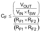
Where
CF is the value of the current limit filter capacitor in F
VOUT is the output voltage of the converter
VIN is the input voltage to the converter
fSW is the converter switching frequency
RF1 and RF2 are the values of the scaling resistors in Ω
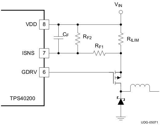 Figure 28. Current Limit Adjustment
NOTE
The current limit resistor and its associated circuitry can be eliminated and the ISNS pin (pin 7) and the VDD pin (pin 8) are shorted. The result of this however, may result in damage to the device or PC board during an overcurrent event.
7.3.6 Calculating the Soft-Start Time
An external capacitor CSS, connected from the SS pin to ground, controls the soft-start interval. An internal charging resistor connected to VDD produces a rising reference voltage which is connected though a 700-mV offset to the reference input of the TPS40200 error amplifier. When the soft-start capacitor voltage (VCSS) is below 150 mV, there is no switching activity. When VCSS rises above the 700 mV offset, the error amplifier starts to follow VSST– 700 mV, and uses this rising voltage as a reference. When VCSS reaches 1.4 V, the internal reference takes over, and further increases have no effect. An advantage of initiating a slow start in this fashion is that the controller cannot overshoot because its output follows a scaled version of the controller reference voltage. A conceptual drawing of the circuit that produces these results is shown in Figure 29. A consequence of the 700 mV offset is that the controller does not start switching until VCSS has risen to 700 mV. The output remains at 0 V during the resulting delay. When VCSS exceeds the 700 mV offset, the TPS40200 output follows the soft-start time constant. Once above 1.4 V, the 700-mV internal reference takes over, and normal operation begins.
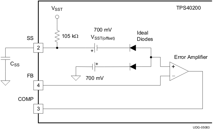 Figure 29. Soft-Start Circuit
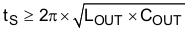
The slow-start time should be longer (slower) than the time constant of the output LC filter. This time constraint may be expressed as described in Equation 5.
The calculation of the soft-start interval is simply the time it takes the RC network to exponentially charge from 0 V to 1.4 V. An internal 105 kΩ charging resistor is connected from the SS pin to VSST. For applications where the voltage is above 8 V, an internal regulator clamps the maximum charging voltage to 8 V.
The result of this is a formula for the start-up time, as shown in Equation 6.
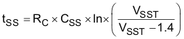
Where
tSS is the required soft-start time in seconds
CSS is the soft-start capacitor value in F
Rc is the internal soft-start charging resistor (105 kΩ nominal)
VSST is the input voltage up to a maximum of 8 V
7.3.7 Voltage Setting and Modulator Gain
Since the input current to the error amplifier is negligible, the feedback impedance can be selected over a wide range. Knowing that the reference voltage is 696 mV, choose a convenient value for R1 and then calculate the value of R2 from Equation 7.
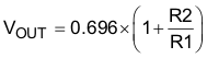
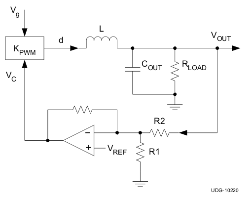 Figure 30. System Gain Elements
The error amplifier has a DC open loop gain of at least 60 dB with a minimum of a 1.5-MHz gain bandwidth product which gives the user flexibility with respect to the type of feedback compensation he uses for his particular application. The gain selected by the user at the crossover frequency is set to provide an over all unity gain for the system. The crossover frequency should be selected so that the error amplifier open-loop gain is high with respect to the required closed-loop gain, ensuring that the amplifier response is determined by the passive feedback elements.
7.4 Device Functional Modes
7.4.1 Operation Near Minimum Input Voltage
The TPS40200 is designed to operate with input voltages above 4.5 V. The typical VDD UVLO threshold is 4.25 V and the device may operate at input voltages down to the UVLO voltage. At input voltages below the actual UVLO voltage, the device will not switch. When VVDD passes the UVLO threshold the device will become active. Switching is enabled and the soft start sequence is initiated. The TPS40200 will ramp up the output voltage at the rate determined by the external capacitor at the soft-start pin.
7.4.2 Operation With SS Pin
The SS pin has a 150 mV threshold which can be used to disable the TPS40200. With SS forced below this threshold voltage the device is disabled and switching is inhibited even if VVDD is above its UVLO threshold. If the SS voltage is allowed to increase above the threshold while VVDD is above its UVLO threshold, the device becomes active. Switching is enabled and the soft start sequence is initiated. The TPS40200 will ramp up the output voltage at the rate determined by the external capacitor at the soft-start pin.